 ChipApex | Global Electronic Components Supplier

SEARCH
Search Product
Search Post
— IC芯片 | 连接器 | 传感器 | 被动器件 —
Search productSearch post
— IC芯片 | 连接器 | 传感器 | 被动器件 —
Consult the customer manager about the wholesale price.
consultation hotline:86-132-6715-2157
email:[email protected]
Contact the product manager for consultation. One-stop consultation is available.
Do you want a lower wholesale price? Please send us your inquiry and we will reply immediately.
The A42MX24-PQG208M is a Field Programmable Gate Array (FPGA) from the Microchip MX family, designed as a high-capacity single-chip ASIC alternative. It features 36,000 system gates and utilizes a 208-pin PQFP package. The device supports mixed-voltage operation with core and I/O voltages of either 5.0V or 3.3V, ensuring PCI compliance. Key performance metrics include a maximum clock frequency of 250 MHz, a 5.6 ns clock-to-out delay, and up to 2.5 kbits of configurable dual-port SRAM. It offers up to 202 user-programmable I/O pins and deterministic timing for complex logic consolidation.
Verify component authenticity through authorized Microchip distributors due to potential counterfeit risks. Confirm RoHS compliance status and check for specific manufacturing date codes relevant to your supply chain requirements. Ensure proper ESD handling procedures are followed during storage and installation to maintain device integrity.
Select this model when a dense logic solution with mixed-voltage compatibility is required. Compare gate counts against similar MX family members if higher capacity is needed. Verify that the 208-pin PQFP package dimensions fit your PCB layout constraints. Consider thermal management requirements given the plastic package construction and operating temperature range.
This component belongs to the Microchip 40MX and 42MX FPGA families, which provide cost-effective design solutions at 5V. These devices are engineered to shorten system design cycles by integrating and consolidating logic from multiple legacy programmable devices into a single chip.
Direct substitutes within the same package may include other variants from the A42MX series such as A42MX16 or A42MX36, depending on specific gate density requirements. Cross-reference pinouts and voltage specifications carefully before substitution.
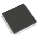 A42MX24-PQG208M

The activity of extra discounts on wholesale prices is in full swing…
Please fill in your contact information and we will send you the latest wholesale price list.






