 ChipApex | Global Electronic Components Supplier

SEARCH
Search Product
Search Post
— IC芯片 | 连接器 | 传感器 | 被动器件 —
Search productSearch post
— IC芯片 | 连接器 | 传感器 | 被动器件 —
Consult the customer manager about the wholesale price.
consultation hotline:86-132-6715-2157
email:[email protected]
Contact the product manager for consultation. One-stop consultation is available.
Do you want a lower wholesale price? Please send us your inquiry and we will reply immediately.
The A42MX36-2BG272 is a high-capacity Field Programmable Gate Array (FPGA) from the Microchip MX family, designed as a single-chip ASIC alternative. It features 54,000 system gates and 1,184 Configurable Logic Blocks (CLBs). The device supports mixed-voltage operation with core and I/O supplies ranging from 3V to 3.6V or 4.75V to 5.25V. It includes up to 2.5 kbits of configurable dual-port SRAM for embedded memory functions. The component utilizes a 272-pin Plastic Ball Grid Array (PBGA) package and offers deterministic, user-controllable timing with up to 100% resource utilization and pin locking capabilities.
Verify the specific suffix code against official Microchip documentation to confirm temperature range and package variant. Confirm current availability status as legacy products may have limited supply chains. Ensure compliance with RoHS and REACH regulations required for your manufacturing environment. Check for any Product Change Notices (PCN) regarding assembly sites or software tool updates that may affect long-term support.
Select this model when 54,000 system gates are required in a BGA form factor. Compare against the A42MX36-2PQG208 if a QFP package is preferred over PBGA. Consider the -3 speed grade variant if lower propagation delays are necessary for high-frequency designs. Verify that the 272-pin footprint matches the target PCB layout constraints.
This component belongs to the Microchip A42MX series, which bridges the gap between CPLDs and larger FPGAs. The MX family is characterized by its non-volatile Flash technology, eliminating the need for external configuration memory. This specific part represents the highest gate count within the standard A42MX36 architecture, offering significant logic density for compact applications.
Publicly confirmed substitute part numbers for this specific package and speed grade were not identified in the provided source data. Consult Microchip's official obsolescence notices for recommended next-generation replacements.
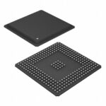 A42MX36-2BG272

The activity of extra discounts on wholesale prices is in full swing…
Please fill in your contact information and we will send you the latest wholesale price list.






