 ChipApex | Global Electronic Components Supplier

SEARCH
Search Product
Search Post
— IC芯片 | 连接器 | 传感器 | 被动器件 —
Search productSearch post
— IC芯片 | 连接器 | 传感器 | 被动器件 —
Consult the customer manager about the wholesale price.
consultation hotline:86-132-6715-2157
email:[email protected]
Contact the product manager for consultation. One-stop consultation is available.
Do you want a lower wholesale price? Please send us your inquiry and we will reply immediately.
The A42MX36-PQ240 is a Field Programmable Gate Array from the Microsemi 42MX family, housed in a PQFP-240 package. It provides 2438 Configurable Logic Blocks (CLBs) and approximately 36,000 system gates. The device supports mixed-voltage operation at 5.0V or 3.3V for both core and I/Os, featuring PCI-compliant inputs and outputs. Key architectural resources include up to 2.5 kbits of configurable dual-port SRAM, fast wide-decode circuitry, and up to 202 user-programmable I/O pins.
Verify the specific speed grade suffix associated with the -PQ240 package variant to ensure timing compliance. Confirm RoHS status and moisture sensitivity level requirements against project specifications. Check for active manufacturing status as legacy FPGA families may face end-of-life transitions.
Select this model when 36,000 system gates and 2438 CLBs are required within a 240-pin plastic quad flatpack form factor. Ensure the design utilizes the available dual-port SRAM capacity if memory functions are needed. Verify that the target voltage domain matches the 5.0V or 3.3V mixed-mode capabilities defined in the datasheet.
This component belongs to the Microsemi 42MX FPGA family, designed as a high-capacity single-chip alternative to ASICs. The family offers scalable gate counts ranging from 3,000 to 54,000 system gates across various packages. The 42MX series is distinguished by its support for mixed-voltage I/O and integrated SRAM resources.
Compatible replacements within the same family include the A42MX36-RQ240 and A42MX36-1RQG240, which offer similar gate counts but differ in package type or speed grade. Verify pinout compatibility and thermal characteristics before substitution.


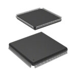 A42MX36-PQ240

The activity of extra discounts on wholesale prices is in full swing…
Please fill in your contact information and we will send you the latest wholesale price list.



