 ChipApex | Global Electronic Components Supplier

SEARCH
Search Product
Search Post
— IC芯片 | 连接器 | 传感器 | 被动器件 —
Search productSearch post
— IC芯片 | 连接器 | 传感器 | 被动器件 —
Consult the customer manager about the wholesale price.
consultation hotline:86-132-6715-2157
email:[email protected]
Contact the product manager for consultation. One-stop consultation is available.
Do you want a lower wholesale price? Please send us your inquiry and we will reply immediately.
The Microsemi A54SX08-2TQ144I is an industrial-grade Field Programmable Gate Array from the SX-A family, housed in a 144-pin Thin Quad Flat Pack. It provides 12,000 system gates and utilizes 0.22 μm / 0.25 μm CMOS antifuse technology. The device supports up to 113 user I/Os and features three global clock networks. It operates within an industrial temperature range of -40°C to +85°C and delivers approximately 25% faster performance than standard speed grades.
Verify the component matches the specified industrial temperature grade (-40°C to +85°C) and the -2 speed grade designation. Confirm the package type is the 144-pin TQFP variant. Ensure the part number suffix corresponds to the correct lead-free or standard packaging requirements as defined by the manufacturer's current ordering guidelines.
Select this device when designs require nonvolatile configuration without external boot ROMs. The -2 speed grade offers higher internal clock frequencies suitable for demanding data path logic. Consider the 113 available user I/Os and the specific mix of combinatorial and sequential resources provided by the sea-of-modules architecture for optimal area utilization.
This component belongs to the Actel SX-A FPGA family, which employs antifuse technology for high-speed, secure, and low-power implementations. The family ranges from 12,000 to 108,000 system gates, offering various package options and speed grades to accommodate diverse design constraints and performance requirements across commercial and industrial sectors.
Direct replacements include other speed grades within the A54SX08A series, such as the standard or -1 variants, if performance margins allow. Higher capacity devices like the A54SX16A may serve as upward-compatible alternatives if additional logic resources are needed, provided pin compatibility or board redesign is acceptable.
Security is ensured because it is difficult to distinguish between programmed and unprogrammed antifuses. Additionally, FuseLock technology prevents reading back the configuration, and hidden security fuses protect against invasive probing.
During power-up or hot-swap, all I/Os are tristated until normal operating conditions are reached. This prevents the device from sinking current or damaging the host system while unpowered.
Yes, in Flexible mode, TDI, TCK, and TDO can function as user I/Os. However, TMS cannot be used as a user I/O in any mode. Dedicated mode reserves all JTAG pins strictly for boundary-scan testing.
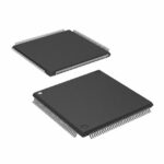 A54SX08-2TQ144I

The activity of extra discounts on wholesale prices is in full swing…
Please fill in your contact information and we will send you the latest wholesale price list.






