 ChipApex | Global Electronic Components Supplier
SEARCH
Search Product
Search Post
— IC芯片 | 连接器 | 传感器 | 被动器件 —
Search productSearch post
— IC芯片 | 连接器 | 传感器 | 被动器件 —
Consult the customer manager about the wholesale price.
consultation hotline:86-132-6715-2157
email:[email protected]
Contact the product manager for consultation. One-stop consultation is available.
Do you want a lower wholesale price? Please send us your inquiry and we will reply immediately.
The A54SX08-2VQG100 is a field-programmable gate array from the Actel SX-A family, fabricated using 0.22 μm / 0.25 μm CMOS antifuse technology. It provides 12,000 system gates, 768 combinatorial cells, and up to 512 dedicated flip-flops. The device operates at a maximum system performance of 250 MHz with internal clock frequencies reaching 350 MHz. It supports mixed-voltage I/O standards including 2.5 V, 3.3 V, and 5 V levels, featuring hot-swap compliant inputs and configurable weak-resistor pull-ups or pull-downs for power-up states.
Verify the specific ordering suffixes against the manufacturer's current datasheet to confirm package type, speed grade, and temperature range compatibility. Ensure that any required configuration software licenses are available prior to procurement. Confirm RoHS compliance status if environmental regulations apply to the target assembly process.
Select this component when designs require nonvolatile configuration without external memory chips. Consider the 12,000 system gate capacity for moderate complexity logic functions. Evaluate the -2 speed grade requirements against the 250 MHz system performance limit. Verify that the 100-pin TQFP package fits the physical constraints of the printed circuit board layout.
This part belongs to the Actel SX-A family of FPGAs, which utilizes antifuse technology for high-speed, secure, and nonvolatile programming. The family ranges from 8,000 to 108,000 system gates, offering scalable solutions for various application densities while maintaining consistent architectural features such as DirectConnect and FastConnect routing resources.
Direct replacements within the same package and pinout include other speed grades of the A54SX08A series, such as the standard or -1 variants, provided timing requirements are met. Cross-family migration to newer Microchip FPGA architectures requires significant redesign due to differences in programming technology and resource architecture.
Security is ensured through the inherent difficulty of distinguishing programmed from unprogrammed antifuses and the Actel FuseLock technology, which prevents reading back the configuration data and protects against invasive probing attacks.
During power-up or hot-swap, all I/Os are tristated by default. The device outputs remain in a high-impedance state until normal operating conditions are reached, preventing damage to the host system.
Yes, in Flexible mode, TDI, TCK, and TDO can function as user I/Os. However, TMS cannot be used as a user I/O in either Dedicated or Flexible modes.


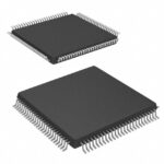 A54SX08-2VQG100
The activity of extra discounts on wholesale prices is in full swing…
Please fill in your contact information and we will send you the latest wholesale price list.



