 ChipApex | Global Electronic Components Supplier

SEARCH
Search Product
Search Post
— IC芯片 | 连接器 | 传感器 | 被动器件 —
Search productSearch post
— IC芯片 | 连接器 | 传感器 | 被动器件 —
Consult the customer manager about the wholesale price.
consultation hotline:86-132-6715-2157
email:[email protected]
Contact the product manager for consultation. One-stop consultation is available.
Do you want a lower wholesale price? Please send us your inquiry and we will reply immediately.
The A54SX08-FGG144 is a Field Programmable Gate Array from the SX-A family, featuring 12,000 system gates and 768 logic modules. It operates with a maximum system frequency of 250 MHz and an internal performance of 350 MHz. The device supports up to 111 user-programmable I/O pins and includes dedicated flip-flops for sequential logic. It utilizes 0.22 μm / 0.25 μm CMOS antifuse technology and supports mixed-voltage operation at 2.5 V, 3.3 V, and 5 V. The component is housed in a 144-pin Fine Pitch Ball Grid Array (FBGA) package.
Verify the specific speed grade suffix associated with the -FGG144 package designation, as standard speed variants exist alongside faster grades within the SX-A family. Confirm that the commercial temperature range aligns with operational requirements. Ensure compatibility with Actel Designer software versions supporting the SX-A architecture for accurate place-and-route implementation.
Select this model when 12,000 system gates and 111 user I/Os are sufficient for the design complexity. Consider the FBGA package for high-density board layouts. Evaluate the 250 MHz system performance against timing constraints. Verify that the 0.22/0.25 μm process technology meets the required power consumption and voltage tolerance specifications for the target application environment.
This component belongs to the Actel SX-A family of FPGAs, which are characterized by their nonvolatile antifuse technology. The family ranges from 12,000 to 108,000 system gates, offering scalable logic density. The SX-A series is designed for low-power, high-performance applications, providing a cost-effective alternative to volatile FPGA solutions while maintaining robust security features against unauthorized access.
Direct functional replacements within the same package and pinout include other speed grades of the A54SX08A series, such as the A54SX08-1FGG144 or A54SX08-2FGG144, provided timing requirements allow for slower performance. Cross-family migration to ProASIC3 or IGLOO devices requires schematic redesign due to architectural differences.

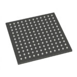 A54SX08-FGG144

The activity of extra discounts on wholesale prices is in full swing…
Please fill in your contact information and we will send you the latest wholesale price list.



