 ChipApex | Global Electronic Components Supplier

SEARCH
Search Product
Search Post
— IC芯片 | 连接器 | 传感器 | 被动器件 —
Search productSearch post
— IC芯片 | 连接器 | 传感器 | 被动器件 —
Consult the customer manager about the wholesale price.
consultation hotline:86-132-6715-2157
email:[email protected]
Contact the product manager for consultation. One-stop consultation is available.
Do you want a lower wholesale price? Please send us your inquiry and we will reply immediately.
The Microsemi A54SX08-VQ100I is an antifuse-based Field Programmable Gate Array (FPGA) from the SX-A family, featuring 12,000 system gates and 768 logic modules. It provides up to 113 user-programmable I/O pins within a 144-pin Thin Quad Flat Pack (TQFP) package. The device supports mixed-voltage operation across 2.5 V, 3.3 V, and 5 V domains with 5 V input tolerance. Operating at industrial temperature grades (-40°C to +85°C), it delivers deterministic performance with internal clock frequencies reaching 350 MHz.
Verify component authenticity through authorized Microchip Technology distributors or direct channels. Confirm that the specific ordering suffix matches the required speed grade and temperature range for your application environment. Ensure compliance with relevant export regulations and environmental standards prior to procurement.
Select this model when nonvolatile configuration and hot-swap capability are required without external boot devices. Consider the 144-pin TQFP package dimensions and thermal dissipation requirements for PCB layout. Evaluate the 113 available I/O count against system interface needs to ensure sufficient pin utilization.
This component belongs to the Actel SX-A family of FPGAs, which utilizes metal-to-metal programmable antifuse technology. The family offers varying capacities ranging from 12,000 to 108,000 system gates, catering to diverse logic density requirements while maintaining consistent architectural features such as DirectConnect and FastConnect routing resources.
Direct functional replacements within the same package and pinout may include other speed grades of the A54SX08A series, provided timing constraints are met. Cross-family migration to newer Microchip FPGA architectures requires significant redesign due to differences in configuration methods and I/O structures.
The SX-A family supports hot-swap operations where supply voltages do not require strict sequencing. All I/Os remain tristated until normal operating conditions are reached, preventing damage to the host system during power transitions.
The device incorporates Actel Secure Programming Technology with FuseLock, which prevents reverse engineering and unauthorized reading of the antifuse configuration. Special security fuses prevent internal probing and overwriting.
Yes, by configuring the Boundary-Scan Testing mode to 'Flexible' in the design software, pins such as TDI, TCK, and TDO can function as user I/Os, although TMS remains reserved for test access port control.
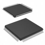 A54SX08-VQ100I

The activity of extra discounts on wholesale prices is in full swing…
Please fill in your contact information and we will send you the latest wholesale price list.






