 ChipApex | Global Electronic Components Supplier
SEARCH
Search Product
Search Post
— IC芯片 | 连接器 | 传感器 | 被动器件 —
Search productSearch post
— IC芯片 | 连接器 | 传感器 | 被动器件 —
Consult the customer manager about the wholesale price.
consultation hotline:86-132-6715-2157
email:[email protected]
Contact the product manager for consultation. One-stop consultation is available.
Do you want a lower wholesale price? Please send us your inquiry and we will reply immediately.
The A54SX08A-PQ208I is a nonvolatile FPGA from the SX-A family, fabricated on 0.22 μm / 0.25 μm CMOS antifuse technology. It provides 12,000 system gates, 768 logic modules (combinatorial cells), and up to 512 dedicated flip-flops. The device supports up to 130 user-programmable I/O pins within a 208-pin Plastic Quad Flat Pack (PQFP) package. It operates at system frequencies up to 250 MHz with internal performance reaching 350 MHz. The component supports mixed-voltage operation across 2.5 V, 3.3 V, and 5 V supplies, features hot-swap compliant I/Os, and includes boundary-scan testing compliance.
Verify the specific ordering suffix against the manufacturer's current datasheet to confirm temperature grade and packaging compliance. The 'I' suffix denotes an industrial temperature range of -40°C to +85°C. Confirm lead-free status if RoHS compliance is required for the assembly process. Ensure the PQFP package dimensions match the target PCB footprint specifications.
Select this device when a nonvolatile configuration is required to eliminate external configuration memory components. The SX-A architecture offers deterministic timing through its sea-of-modules design with DirectConnect and FastConnect routing resources. Consider the 12,000 gate capacity and 130 I/O limit for mid-complexity logic integration tasks requiring fast time-to-market.
This component belongs to the Microsemi (formerly Actel) SX-A family of FPGAs. The family utilizes antifuse technology rather than SRAM-based configuration, providing inherent security and zero standby power. The A54SX08A represents the entry-level capacity in the series, offering a balance of logic density and pin count suitable for consolidating multiple CPLD or PAL functions into a single chip.
Direct functional replacements within the same package and pinout include other speed grades of the A54SX08A series, such as the standard speed variant or faster grades like the A54SX08A-1PQ208I, provided timing requirements are met. Cross-family migration to newer Microchip PolarFire or SmartFusion devices requires significant architectural redesign due to differences in configuration technology and I/O structures.
The SX-A family uses a patented metal-to-metal antifuse interconnect that forms permanent low-impedance connections. Combined with local routing resources like DirectConnect and FastConnect, the place-and-route software can minimize signal propagation delays, ensuring highly predictable performance.
During power-up or hot-swap, all I/Os are tristated by default. The VCCA and VCCI supplies do not require sequencing and can be powered in any order. This prevents the device from sinking current or damaging the host system when plugged into an active circuit.
Yes, in Flexible mode, TDI, TCK, and TDO can function as user I/Os or BST pins. However, TMS cannot be used as a user I/O in either Dedicated or Flexible modes. In Dedicated mode, all JTAG pins are reserved strictly for Boundary-Scan Testing.

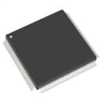 A54SX08A-PQ208I
The activity of extra discounts on wholesale prices is in full swing…
Please fill in your contact information and we will send you the latest wholesale price list.




