 ChipApex | Global Electronic Components Supplier
SEARCH
Search Product
Search Post
— IC芯片 | 连接器 | 传感器 | 被动器件 —
Search productSearch post
— IC芯片 | 连接器 | 传感器 | 被动器件 —
Consult the customer manager about the wholesale price.
consultation hotline:86-132-6715-2157
email:[email protected]
Contact the product manager for consultation. One-stop consultation is available.
Do you want a lower wholesale price? Please send us your inquiry and we will reply immediately.
The A54SX16-PQG208I is a nonvolatile FPGA from the SX-A family, fabricated on 0.22 μm / 0.25 μm CMOS antifuse technology. It provides 24,000 system gates and 1,452 logic modules (CLBs). The device supports up to 175 user-programmable I/O pins in a 208-pin PQFP package. It operates within an industrial temperature range of -40°C to +85°C. The architecture includes three global clock networks and features hot-swap compliant I/Os with mixed-voltage support for 2.5 V, 3.3 V, and 5 V standards.
Verify the component origin as Microsemi Corporation, noting that Actel was acquired by Microsemi. Confirm the package type is Plastic Quad Flat Pack (PQFP) with 208 pins. Ensure the suffix 'I' corresponds to the specified industrial temperature grade. Check for RoHS compliance status if required by local regulations, as standard packaging may differ from lead-free variants.
Select this model when 24,000 system gates and 1,452 CLBs are sufficient for the design. The PQG208I variant is appropriate for surface-mount assembly requiring industrial temperature stability. Consider the A54SX16A series if automotive or military temperature grades are needed instead of the industrial grade. Verify that the 175 available user I/Os meet the interface requirements.
This part belongs to the Actel SX-A family of FPGAs, which were originally manufactured by Actel Corporation before its acquisition by Microsemi. The SX-A family is characterized by its high-density antifuse technology and optimized routing resources like DirectConnect and FastConnect. This specific device represents a mid-range capacity option within the family, balancing logic density with I/O availability.
Direct replacements include other devices from the A54SX16A series with different speed grades or packages, such as A54SX16A-PQG208C for commercial temperature or A54SX16A-CQG208I for ceramic packaging. Cross-family migration to ProASIC3 or IGLOO devices requires architectural redesign due to differences in nonvolatile technology and logic structure.
The SX-A family architecture supports internal clock frequencies up to 350 MHz, enabling fast execution of complex logic functions.
The device is power-up/down friendly, meaning no sequencing is required for supply voltages. VCCA and VCCI can be powered up or down in any order.
Yes, in Flexible mode, TDI, TCK, and TDO can function as user I/Os. However, TMS cannot be employed as a user I/O in either Dedicated or Flexible modes.
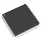 A54SX16-PQG208I
The activity of extra discounts on wholesale prices is in full swing…
Please fill in your contact information and we will send you the latest wholesale price list.






