 ChipApex | Global Electronic Components Supplier
SEARCH
Search Product
Search Post
— IC芯片 | 连接器 | 传感器 | 被动器件 —
Search productSearch post
— IC芯片 | 连接器 | 传感器 | 被动器件 —
Consult the customer manager about the wholesale price.
consultation hotline:86-132-6715-2157
email:[email protected]
Contact the product manager for consultation. One-stop consultation is available.
Do you want a lower wholesale price? Please send us your inquiry and we will reply immediately.
The A54SX16-VQ100I is a Field Programmable Gate Array from the Microsemi SX-A family, fabricated using 0.22 μm / 0.25 μm CMOS antifuse technology. It provides 24,000 system gates and 1,452 configurable logic blocks (CLBs). The device supports up to 81 user-programmable I/O pins within a 100-pin Thin Quad Flat Pack (TQFP) package. It features three global clock networks and operates at maximum internal frequencies of 350 MHz with standard speed grades.
Verify the specific ordering suffix against the manufacturer's official datasheet to confirm temperature grade and packaging compliance. Confirm that the component matches the exact pin count and gate density specifications required for the target application design.
Select this model based on the requirement for 24,000 system gates and 100-pin TQFP packaging. Ensure the design utilizes the available 81 user I/Os and leverages the three global clock networks provided by the SX-A architecture for optimal performance.
This component belongs to the Actel SX-A family of FPGAs, which are designed for cost-effective, low-power applications. The family utilizes antifuse technology to provide secure, nonvolatile programming capabilities with high-speed performance characteristics suitable for complex logic implementations.
Compatible alternatives within the same family include the A54SX16A series variants with different speed grades or package options. Verify functional equivalence regarding gate count and I/O availability before substitution.
The device supports internal clock frequencies up to 350 MHz.
The A54SX16-VQ100I includes three global clock networks: one hardwired HCLK and two routed clocks (CLKA and CLKB).
Yes, the I/Os are configured to be hot-swappable, except for 3.3 V PCI configurations.


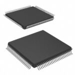 A54SX16-VQ100I
The activity of extra discounts on wholesale prices is in full swing…
Please fill in your contact information and we will send you the latest wholesale price list.




