 ChipApex | Global Electronic Components Supplier
SEARCH
Search Product
Search Post
— IC芯片 | 连接器 | 传感器 | 被动器件 —
Search productSearch post
— IC芯片 | 连接器 | 传感器 | 被动器件 —
Consult the customer manager about the wholesale price.
consultation hotline:86-132-6715-2157
email:[email protected]
Contact the product manager for consultation. One-stop consultation is available.
Do you want a lower wholesale price? Please send us your inquiry and we will reply immediately.
The A54SX16A-FGG256M is a Field Programmable Gate Array from the SX-A family, featuring 24,000 system gates and 180 user-programmable I/O pins. It utilizes 0.22 μm / 0.25 μm CMOS antifuse technology with a standard operating voltage of 2.5 V (range 2.25 V to 2.75 V). The device supports a maximum system performance frequency of 250 MHz and an internal clock frequency of 350 MHz. It is housed in a 256-pin Fine Pitch Ball Grid Array (FBGA) package and offers an industrial temperature grade range of -40°C to +85°C.
Verify the specific ordering suffix 'M' against official Microchip documentation to confirm its exact definition regarding packaging or qualification. Confirm current availability status as legacy antifuse products may have limited production runs. Ensure compliance with RoHS directives if required by the application environment.
Select this device when 24,000 system gates and 180 I/Os are sufficient for the design. Consider the FBGA256 package for high-density board layouts. Verify that the 250 MHz system speed meets the timing constraints. Check if the industrial temperature range (-40°C to +85°C) aligns with environmental requirements.
This component belongs to the Actel SX-A family of FPGAs, which were originally developed by Actel Corporation and later acquired by Microsemi (now part of Microchip Technology). The SX-A series is characterized by its antifuse-based nonvolatile architecture, offering high reliability and security compared to SRAM-based FPGAs.
Direct pin-compatible replacements within the same package and speed grade are not explicitly listed in the provided datasheet. Designers should evaluate other devices in the A54SX16A series with different speed grades or temperature codes, or consider higher-capacity devices like the A54SX32A if resource expansion is acceptable.
HCLK is a hardwired clock network connected directly to the clock select multiplexor in each R-cell, providing the fastest propagation path but cannot be connected to combinatorial logic. CLKA and CLKB are routed global clocks that can be sourced from external pins or internal logic and can drive both sequential and combinational cells.
FuseLock prevents reverse engineering and unauthorized reading of the design. It uses special security fuses hidden throughout the fabric to prevent internal probing and overwriting, making invasive and noninvasive attacks ineffective against the antifuse FPGA.
No, unused I/O pins must not be left floating. They should be configured as tristate outputs by the software or tied to a defined logic level (Low or High) on the board to ensure proper operation and prevent excessive current draw or noise.
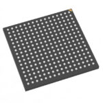 A54SX16A-FGG256M
The activity of extra discounts on wholesale prices is in full swing…
Please fill in your contact information and we will send you the latest wholesale price list.





