 ChipApex | Global Electronic Components Supplier
SEARCH
Search Product
Search Post
— IC芯片 | 连接器 | 传感器 | 被动器件 —
Search productSearch post
— IC芯片 | 连接器 | 传感器 | 被动器件 —
Consult the customer manager about the wholesale price.
consultation hotline:86-132-6715-2157
email:[email protected]
Contact the product manager for consultation. One-stop consultation is available.
Do you want a lower wholesale price? Please send us your inquiry and we will reply immediately.
The A54SX16A-FTQG100 is a Field Programmable Gate Array from the SX-A family, fabricated using 0.22 μm / 0.25 μm CMOS antifuse technology. It provides 24,000 system gates and 1,452 logic modules within a 100-pin Thin Quad Flat Pack (TQFP) package. The device supports up to 81 user-programmable I/O pins and features three global clock networks. It operates with internal clock frequencies up to 350 MHz and system performance up to 250 MHz. The component supports mixed-voltage operation at 2.5 V, 3.3 V, and 5 V, ensuring compatibility with various interface standards.
Verify the specific speed grade suffix associated with the FTQG100 designation, as standard SX-A ordering typically uses F, Std, -1, or -2. Confirm that the Industrial temperature grade (I) matches the required operational range of -40°C to +85°C. Ensure the RoHS compliance status aligns with current environmental regulations for the target market.
Select this device when 24,000 system gates are sufficient for the design complexity. Consider the TQFP-100 package constraints regarding pin count and thermal dissipation. Evaluate if the 81 available user I/Os meet the interface requirements. Verify that the antifuse programming infrastructure is compatible with the chosen design tools.
This component belongs to the Actel SX-A family of FPGAs, which was later acquired by Microchip Technology. The SX-A series is characterized by its high-speed antifuse technology and deterministic performance. The A54SX16A variant specifically targets designs requiring moderate logic density with high-speed processing capabilities.
Direct replacements include other speed grades within the A54SX16A series such as A54SX16A-F, A54SX16A-Std, or A54SX16A-1, provided the package and temperature grade match. Cross-family migration to newer Microchip FPGA architectures may require significant design rework due to architectural differences.
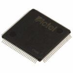 A54SX16A-FTQG100
The activity of extra discounts on wholesale prices is in full swing…
Please fill in your contact information and we will send you the latest wholesale price list.





