 ChipApex | Global Electronic Components Supplier
SEARCH
Search Product
Search Post
— IC芯片 | 连接器 | 传感器 | 被动器件 —
Search productSearch post
— IC芯片 | 连接器 | 传感器 | 被动器件 —
Consult the customer manager about the wholesale price.
consultation hotline:86-132-6715-2157
email:[email protected]
Contact the product manager for consultation. One-stop consultation is available.
Do you want a lower wholesale price? Please send us your inquiry and we will reply immediately.
The A54SX16P-2TQ144I is a Field Programmable Gate Array from the Actel SX-A family, fabricated using 0.22 μm / 0.25 μm CMOS antifuse technology. It provides 1,452 logic modules and 24,000 system gates within a 144-pin Thin Quad Flat Pack (TQFP) package. The device supports a maximum internal clock frequency of 350 MHz and operates at an industrial temperature range of -40°C to +85°C. Key specifications include up to 113 user-programmable I/O pins, dedicated global clock networks, and support for mixed-voltage operation including 2.5 V, 3.3 V, and 5 V standards.
Verify the specific ordering suffix against the manufacturer's current datasheet to confirm package type, speed grade, and temperature rating. Ensure compatibility with existing PCB footprints for the TQFP-144 package. Confirm RoHS compliance status if required by assembly specifications. Check for any discontinued status or alternative recommendations from Microchip Technology before finalizing procurement.
Select this device when a nonvolatile FPGA with high-speed deterministic timing is required. The SX-A architecture offers full resource utilization and pin-locking capabilities. Consider the available speed grades and temperature ranges to match application constraints. Evaluate the I/O voltage flexibility for mixed-signal interfaces. Verify that the antifuse programming infrastructure aligns with the design workflow.
This component belongs to the Actel SX-A family of FPGAs, which are known for their low-power consumption and high-density logic capabilities. The SX-A series utilizes antifuse technology, distinguishing it from volatile SRAM-based FPGAs. This family includes various gate counts and package options to suit different design complexities and form factor requirements.
Direct replacements may not exist due to the proprietary antifuse technology. Evaluate devices from other manufacturers offering similar gate counts and I/O configurations. Ensure that the replacement supports the required speed grades and temperature ranges. Verify pinout compatibility or plan for adapter solutions if physical dimensions differ significantly.
The antifuse technology provides a nonvolatile, single-chip solution that eliminates the need for external configuration memory and offers inherent security against reverse engineering.
The I/Os are configured to be hot-swappable, meaning they tristate during power-up/down, allowing the device to be plugged into an active system without causing damage or degrading reliability.
The architecture uses DirectConnect and FastConnect routing resources, which provide predictable signal propagation paths with minimal antifuse usage, ensuring fast and consistent performance.
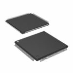 A54SX16P-2TQ144I
The activity of extra discounts on wholesale prices is in full swing…
Please fill in your contact information and we will send you the latest wholesale price list.






