 ChipApex | Global Electronic Components Supplier
SEARCH
Search Product
Search Post
— IC芯片 | 连接器 | 传感器 | 被动器件 —
Search productSearch post
— IC芯片 | 连接器 | 传感器 | 被动器件 —
Consult the customer manager about the wholesale price.
consultation hotline:86-132-6715-2157
email:[email protected]
Contact the product manager for consultation. One-stop consultation is available.
Do you want a lower wholesale price? Please send us your inquiry and we will reply immediately.
The A54SX16P-TQG144 is a Field Programmable Gate Array from the Actel SX-A family, fabricated using 0.22 μm / 0.25 μm CMOS antifuse technology. It provides 24,000 system gates and contains 1,452 logic modules (CLBs). The device supports up to 360 user-programmable I/O pins and includes dedicated flip-flops for sequential logic. It operates with internal clock frequencies up to 350 MHz and delivers 250 MHz system performance. The component is housed in a 144-pin Thin Quad Flat Pack (TQFP) package.
Verify the specific ordering suffix against the manufacturer's current datasheet to confirm temperature grade and packaging compliance. The 'P' designation indicates a Plastic Quad Flat Pack variant, while 'TQ' specifies the Thin Quad Flat Pack form factor. Ensure the selected speed grade matches the required system timing constraints before finalizing procurement orders.
Select this device when a nonvolatile FPGA with high-speed antifuse technology is required. The SX-A architecture offers 100% pin-locking capability and full resource utilization. Consider the available speed grades and temperature ranges to ensure compatibility with the target application environment and performance requirements.
This component belongs to the Actel SX-A family of FPGAs, which are designed for cost-effective, low-power, and high-performance applications. The family utilizes antifuse technology to provide robust security and deterministic performance. The A54SX16 model represents a mid-range capacity within the series, balancing logic density with I/O flexibility.
Direct replacements within the same package and pinout include other speed grades of the A54SX16A series, such as A54SX16A-TQG144I or A54SX16A-TQG144M, provided the timing requirements are met. Cross-family migration to Microchip PolarFire or IGLOO devices requires schematic redesign due to architectural differences.
Reverse engineering is prevented because it is difficult to distinguish between programmed and unprogrammed antifuses. Additionally, FuseLock technology hides security fuses throughout the fabric, making invasive and noninvasive attacks ineffective.
All I/Os are configured to be hot-swappable and tristated during power-up/down. Supply voltages VCCA and VCCI do not need to be stable or sequenced, allowing them to power up in any order.
Yes, if the 'Reserve JTAG' option is unchecked in the design software, the TDI, TCK, and TDO pins can function as user I/Os or BST pins depending on the TAP controller state. TMS cannot be used as a user I/O.
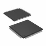 A54SX16P-TQG144
The activity of extra discounts on wholesale prices is in full swing…
Please fill in your contact information and we will send you the latest wholesale price list.






