 ChipApex | Global Electronic Components Supplier
SEARCH
Search Product
Search Post
— IC芯片 | 连接器 | 传感器 | 被动器件 —
Search productSearch post
— IC芯片 | 连接器 | 传感器 | 被动器件 —
Consult the customer manager about the wholesale price.
consultation hotline:86-132-6715-2157
email:[email protected]
Contact the product manager for consultation. One-stop consultation is available.
Do you want a lower wholesale price? Please send us your inquiry and we will reply immediately.
The A54SX32-TQ144 is a Field Programmable Gate Array from the Actel SX-A family, fabricated on 0.22 μm / 0.25 μm CMOS antifuse technology. It provides 48,000 system gates and 2,880 logic modules (CLBs). The device features up to 111 user-programmable I/Os in the TQFP-144 package and supports mixed-voltage operation at 2.5 V, 3.3 V, and 5 V with 5 V input tolerance. It achieves internal performance of 350 MHz and system performance of 250 MHz. The architecture includes three global clock networks and dedicated flip-flops for deterministic timing.
Verify the specific speed grade suffix required for the target frequency, as blank indicates standard speed. Confirm temperature grade availability for the intended environment. Check current manufacturing status as older antifuse families may have limited supply channels. Ensure ECAD models match the TQFP-144 footprint dimensions precisely.
Select this device when 48,000 system gates are sufficient for the design complexity. Consider the TQFP-144 package if surface mount space allows but BGA options are unavailable. Evaluate the need for 5V tolerance if interfacing with legacy logic. Verify that the 250 MHz system performance meets the maximum clock requirements of the application logic.
This component belongs to the Actel SX-A family of FPGAs, which transitioned to Microchip Technology following acquisition. The SX-A series is characterized by its antifuse-based nonvolatile configuration, distinguishing it from SRAM-based FPGAs that require external configuration memory. The A54SX32 variant sits between the A54SX16A and A54SX72A in terms of logic capacity within the standard commercial/industrial lineup.
Direct functional replacements within the same package and gate count are not explicitly listed in the provided datasheet excerpts. Designers migrating from this part should evaluate newer Microchip PolarFire or IGLOO families, noting significant architectural differences between antifuse and flash/SRAM technologies.
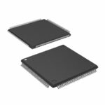 A54SX32-TQ144
The activity of extra discounts on wholesale prices is in full swing…
Please fill in your contact information and we will send you the latest wholesale price list.






