 ChipApex | Global Electronic Components Supplier
SEARCH
Search Product
Search Post
— IC芯片 | 连接器 | 传感器 | 被动器件 —
Search productSearch post
— IC芯片 | 连接器 | 传感器 | 被动器件 —
Consult the customer manager about the wholesale price.
consultation hotline:86-132-6715-2157
email:[email protected]
Contact the product manager for consultation. One-stop consultation is available.
Do you want a lower wholesale price? Please send us your inquiry and we will reply immediately.
The A54SX32-TQ144I is a Field Programmable Gate Array from the Actel SX-A family, fabricated using 0.22 μm / 0.25 μm CMOS antifuse technology. It provides 48,000 system gates and 2,880 logic modules (combinatorial cells). The device supports up to 249 user-programmable I/O pins and includes dedicated flip-flops for sequential logic. It operates with internal clock frequencies up to 350 MHz and delivers 250 MHz system performance. The component is housed in a 144-pin Thin Quad Flat Pack (TQFP) package and is rated for industrial temperature grades ranging from -40°C to +85°C.
Verify the specific ordering suffix against current manufacturer documentation to confirm package type and temperature grade. Confirm availability status as older speed grades may be discontinued. Ensure design tools support the SX-A antifuse programming process before procurement.
Select this model for applications requiring high-speed logic with fixed antifuse configuration rather than volatile SRAM-based FPGAs. Consider the 144-pin TQFP package constraints for PCB layout. Verify that the 249 I/O count meets interface requirements and check if higher capacity devices like the A54SX72A are needed for larger designs.
This component belongs to the Actel SX-A family of nonvolatile FPGAs. It utilizes permanent antifuse technology which eliminates the need for external configuration memory. The family offers various gate counts and packages, positioning these devices as cost-effective alternatives to traditional CPLDs or gate arrays for high-density logic applications.
Direct pin-compatible replacements within the same package and speed grade should be verified through official Microchip/Actel cross-reference lists. Note that newer FPGA families may require significant architectural redesign due to differences in logic blocks and routing structures.
The architecture uses patented metal-to-metal programmable antifuses and optimized routing resources like DirectConnect and FastConnect, ensuring consistent signal propagation delays regardless of the programmed design.
HCLK is a hardwired clock network that provides a fast propagation path directly to R-cell multiplexors. It cannot be connected to combinatorial logic and must be tied High or Low if unused to prevent floating inputs.
Yes, in Flexible mode, TDI, TCK, and TDO can function as user I/Os. However, TMS cannot be used as a user I/O in any mode, and TRST functions as a reset pin only when specifically reserved in software.
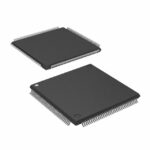 A54SX32-TQ144I
The activity of extra discounts on wholesale prices is in full swing…
Please fill in your contact information and we will send you the latest wholesale price list.






