ChipApex | Global Electronic Components Supplier
SEARCH
Search Product
Search Post
— IC芯片 | 连接器 | 传感器 | 被动器件 —
Search productSearch post
— IC芯片 | 连接器 | 传感器 | 被动器件 —
Consult the customer manager about the wholesale price.
consultation hotline:86-132-6715-2157
email:[email protected]
Contact the product manager for consultation. One-stop consultation is available.
Do you want a lower wholesale price? Please send us your inquiry and we will reply immediately.
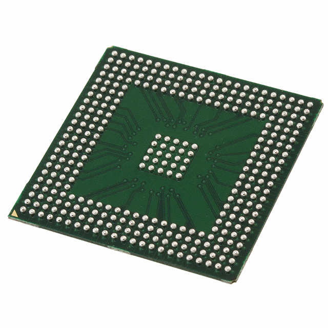
The A54SX32A-FBGG329 is a Field Programmable Gate Array from the Microchip SX-A family, utilizing antifuse technology. It features 48,000 system gates and 2,880 logic modules within a 329-pin Fine Pitch Ball Grid Array (FBGA) package. The device supports up to 249 user-programmable I/O pins and operates at a maximum frequency of 172 MHz. It functions with supply voltages between 2.25 V and 2.75 V and is rated for commercial temperature ranges.
Verify the specific speed grade suffix associated with the FBGG329 package variant to ensure it meets the required timing constraints for your design. Confirm that the component matches the intended temperature grade, as the standard commercial grade covers 0°C to +70°C. Check for any relevant Product Change Notifications regarding manufacturing updates or packaging changes before finalizing procurement orders.
Select this model when a high pin count in a compact BGA footprint is required alongside significant logic density. Ensure the design utilizes the available global clock networks effectively. Consider the nonvolatile nature of the antifuse architecture if reprogramming flexibility is not needed, as it offers inherent security against reverse engineering compared to volatile SRAM-based FPGAs.
This component belongs to the SX-A family of FPGAs, which are fabricated using 0.22 μm / 0.25 μm CMOS antifuse technology. The family provides a cost-effective, low-power solution for integrating CPLD and FPGA functionality into a single chip. The A54SX32A specifically targets applications needing moderate logic capacity with high-speed performance.
Publicly confirmed substitute part numbers are not available in the provided documentation. Designers should consult official Microchip resources for legacy support or alternative device recommendations within the same product family.


 A54SX32A-FBGG329
The activity of extra discounts on wholesale prices is in full swing…
Please fill in your contact information and we will send you the latest wholesale price list.