 ChipApex | Global Electronic Components Supplier
SEARCH
Search Product
Search Post
— IC芯片 | 连接器 | 传感器 | 被动器件 —
Search productSearch post
— IC芯片 | 连接器 | 传感器 | 被动器件 —
Consult the customer manager about the wholesale price.
consultation hotline:86-132-6715-2157
email:[email protected]
Contact the product manager for consultation. One-stop consultation is available.
Do you want a lower wholesale price? Please send us your inquiry and we will reply immediately.
The A54SX32A-FFG144 is a Field Programmable Gate Array from the SX-A family, manufactured by Microsemi. It features 48,000 system gates and 2,880 logic modules within a 144-pin Fine Pitch Ball Grid Array package. The device supports up to 111 user-programmable I/O pins and includes dedicated flip-flops for sequential logic implementation. It operates with a maximum clock frequency of 172 MHz and utilizes 0.22 μm / 0.25 μm CMOS antifuse technology. The component provides mixed-voltage I/O support for 2.5 V, 3.3 V, and 5 V standards.
Verify the specific speed grade suffix associated with the FFG144 package to ensure compliance with target timing constraints. Confirm the temperature range designation matches the operational environment requirements. Check for RoHS compliance markings if environmental regulations apply to the final assembly process.
Select this model when 48,000 system gates are required in a compact 144-pin footprint. Ensure the design fits within the 2,880 CLB limit and available I/O count. Consider the standard speed grade performance against application latency needs before choosing faster or slower variants.
This component belongs to the Actel SX-A FPGA family, which utilizes antifuse technology for permanent programming. The SX-A series is designed for applications requiring high reliability and security, distinguishing it from volatile SRAM-based FPGAs. It serves as a cost-effective alternative to complex gate arrays for fixed-function logic implementations.
Compatible packages include the A54SX32A-TQG144 (TQFP) and A54SX32A-FBGG329 (FBGA). Verify pinout compatibility and thermal characteristics when substituting different package types within the same device family.
No, the device uses nonvolatile antifuse technology, eliminating the need for external configuration bitstreams or memory devices.
The SX-A family architecture supports internal clock frequencies up to 350 MHz, though the specific speed grade determines the actual system performance.
No, unused I/O pins must be configured as tristate outputs or tied to a defined logic level to prevent undefined states and potential current leakage.
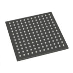 A54SX32A-FFG144
The activity of extra discounts on wholesale prices is in full swing…
Please fill in your contact information and we will send you the latest wholesale price list.






