ChipApex | Global Electronic Components Supplier
SEARCH
Search Product
Search Post
— IC芯片 | 连接器 | 传感器 | 被动器件 —
Search productSearch post
— IC芯片 | 连接器 | 传感器 | 被动器件 —
Consult the customer manager about the wholesale price.
consultation hotline:86-132-6715-2157
email:[email protected]
Contact the product manager for consultation. One-stop consultation is available.
Do you want a lower wholesale price? Please send us your inquiry and we will reply immediately.
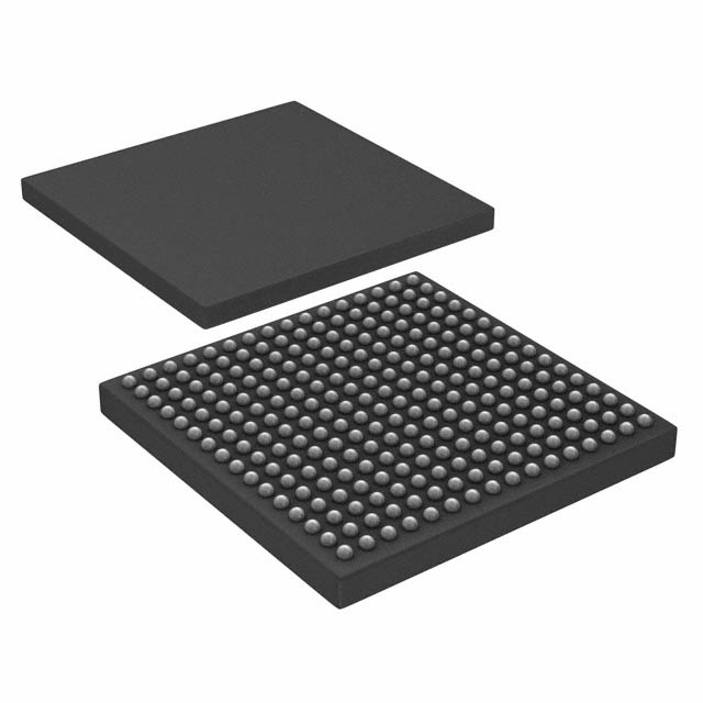
The A54SX32A-FFGG256 is a Field Programmable Gate Array from the SX-A family, fabricated using 0.22 μm / 0.25 μm CMOS antifuse technology. It provides 48,000 system gates and 2,880 logic modules (CLBs). The device supports up to 203 user-programmable I/O pins and includes 1,080 dedicated flip-flops. It operates with internal clock frequencies up to 350 MHz and delivers 250 MHz system performance. The component utilizes a 256-pin Fine Pitch Ball Grid Array (FBGA) package.
Verify the specific speed grade suffix associated with the FFGG256 package variant, as standard speed grades are designated by blank or -1/-2 suffixes. Confirm RoHS compliance status through the 'G' ordering suffix if required. Ensure the design software reserves JTAG pins correctly for boundary-scan testing compliance. Check for any discontinuance notifications regarding the SX-A family prior to final procurement.
Select this device when 48,000 system gates and 203 I/Os are required in a 256-pin FBGA form factor. Choose appropriate speed grades based on the 250 MHz system performance target. Consider the automotive or military temperature grades if operating conditions exceed commercial limits. Verify that the antifuse-based nonvolatility meets the security requirements for the application.
This component belongs to the Actel SX-A FPGA family, which was later acquired by Microchip Technology. The SX-A series is characterized by its antifuse technology, offering high performance and security compared to volatile SRAM-based FPGAs. The A54SX32A represents the mid-range capacity within this portfolio, bridging the gap between smaller A54SX16A and larger A54SX72A devices.
Publicly confirmed substitute part numbers are not available in the provided documentation. Designers migrating from other families should consult Microchip's official migration guides for equivalent gate counts and pin-compatible options within the current product line.
 A54SX32A-FFGG256
The activity of extra discounts on wholesale prices is in full swing…
Please fill in your contact information and we will send you the latest wholesale price list.