 ChipApex | Global Electronic Components Supplier
SEARCH
Search Product
Search Post
— IC芯片 | 连接器 | 传感器 | 被动器件 —
Search productSearch post
— IC芯片 | 连接器 | 传感器 | 被动器件 —
Consult the customer manager about the wholesale price.
consultation hotline:86-132-6715-2157
email:[email protected]
Contact the product manager for consultation. One-stop consultation is available.
Do you want a lower wholesale price? Please send us your inquiry and we will reply immediately.
The A54SX32A-FG484 is a Field Programmable Gate Array from the SX-A family, featuring 48,000 system gates and 2880 logic modules. It supports up to 249 user-programmable I/O pins and includes 1,980 dedicated flip-flops. The device operates with a maximum system performance of 250 MHz and an internal clock frequency of 350 MHz. It utilizes 0.22 μm / 0.25 μm CMOS antifuse technology and supports mixed-voltage operation at 2.5 V, 3.3 V, and 5 V with 5 V input tolerance. The component is housed in a 484-pin Fine Pitch Ball Grid Array (FBGA) package.
Verify the specific speed grade suffix associated with the FG484 package variant, as standard and faster grades exist within the A54SX32A series. Confirm that the ordering suffix indicates the correct temperature range, typically Industrial or Automotive for this package type. Ensure compatibility with Actel Designer software versions supporting the SX-A architecture for programming and place-and-route operations.
Select this model when 48,000 system gates and 249 I/Os are required in a high-density BGA form factor. Consider the SX-A family's nonvolatile antifuse technology if single-chip integration and security against reverse engineering are priorities. Evaluate the 250 MHz system performance limit against design timing constraints before choosing over higher-capacity devices like the A54SX72A.
This component belongs to the Actel SX-A FPGA family, which bridges the gap between CPLDs and larger FPGAs. The SX-A line is characterized by its high-speed metal-to-metal antifuse interconnects and support for mixed-voltage I/O standards. It serves as a cost-effective solution for designs previously implemented using multiple discrete logic components or gate arrays.
Direct replacements include other speed grades of the A54SX32A in the FG484 package, such as A54SX32A-1FG484 or A54SX32A-2FG484, depending on required timing performance. Cross-family migration to SmartFusion2 or IGLOO2 may be necessary for long-term availability, though architectural differences require significant design rework.
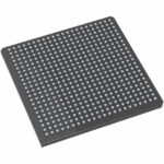 A54SX32A-FG484
The activity of extra discounts on wholesale prices is in full swing…
Please fill in your contact information and we will send you the latest wholesale price list.






