ChipApex | Global Electronic Components Supplier
SEARCH
Search Product
Search Post
— IC芯片 | 连接器 | 传感器 | 被动器件 —
Search productSearch post
— IC芯片 | 连接器 | 传感器 | 被动器件 —
Consult the customer manager about the wholesale price.
consultation hotline:86-132-6715-2157
email:[email protected]
Contact the product manager for consultation. One-stop consultation is available.
Do you want a lower wholesale price? Please send us your inquiry and we will reply immediately.
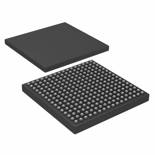
The A54SX32A-FGG256A is an automotive-grade Field Programmable Gate Array (FPGA) from the SX-A family, manufactured by Microchip Technology. It features a sea-of-modules architecture with 48,000 typical system gates and 2,880 combinatorial cells. The device supports up to 203 user I/Os and includes 1,080 dedicated flip-flops. It operates within a voltage range of 2.25 V to 2.75 V and functions across an extended temperature range of -40°C to +125°C. Packaged in a 256-pin Fine Pitch Ball Grid Array (FBGA), it utilizes a 0.22µ CMOS process technology.
Verify the specific ordering suffix 'G' indicates RoHS compliant packaging as defined in the datasheet. Confirm the package type corresponds to the 256-pin FBGA variant. Ensure design tools support the SX-A family architecture for proper configuration. Check for any relevant Product Change Notifications regarding manufacturing or software updates.
Select this component when automotive temperature grades (-40°C to +125°C) are required alongside nonvolatile configuration. Consider the 48,000 gate capacity and 203 I/O limits for system complexity. Evaluate the need for hot-swap capability and JTAG boundary scan testing. Compare against other SX-A devices if different gate counts or package sizes are needed.
This part belongs to the Actel SX-A Automotive Family FPGAs, which utilize a sea-of-modules architecture optimized for fast signal propagation. The family includes variants like A54SX08A, A54SX16A, and A54SX72A, differing primarily in gate count and I/O availability. The SX-A series is designed to reduce design time and power consumption compared to previous generations.
Publicly confirmed substitute part numbers are not available in the provided documentation. Designers should consult Microchip Technology for current equivalent recommendations or migration paths from discontinued or alternative FPGA families.
During power-up, down, or partial up/down, all I/Os are tristated. This allows the device to be plugged into an electrically active system without degrading reliability or causing damage, as output pins remain high impedance until normal operating conditions are reached.
The device uses Actel’s FuseLock™ technology, which prevents unauthorized reading of the antifuse contents. Special security fuses prevent internal probing and overwriting, making reverse engineering virtually impossible due to the difficulty in distinguishing programmed from unprogrammed antifuses.
Yes, in Flexible mode, TDI, TCK, and TDO may function as user I/Os or BST pins. However, TMS cannot be employed as a user I/O in either Dedicated or Flexible mode. In Dedicated mode, all JTAG pins are reserved for BST.

 A54SX32A-FGG256A
The activity of extra discounts on wholesale prices is in full swing…
Please fill in your contact information and we will send you the latest wholesale price list.