 ChipApex | Global Electronic Components Supplier
SEARCH
Search Product
Search Post
— IC芯片 | 连接器 | 传感器 | 被动器件 —
Search productSearch post
— IC芯片 | 连接器 | 传感器 | 被动器件 —
Consult the customer manager about the wholesale price.
consultation hotline:86-132-6715-2157
email:[email protected]
Contact the product manager for consultation. One-stop consultation is available.
Do you want a lower wholesale price? Please send us your inquiry and we will reply immediately.
The A54SX32A-TQG100 is a Field Programmable Gate Array from the Microchip SX-A family, featuring 48,000 system gates and 2,880 logic modules. It supports up to 81 user-programmable I/O pins within a 100-pin Thin Quad Flat Pack (TQFP) package. The device operates on a 0.22 μm / 0.25 μm CMOS antifuse process, enabling internal clock frequencies up to 350 MHz and system performance of 250 MHz. It accommodates mixed-voltage I/O standards including 2.5 V, 3.3 V, and 5 V with 5 V input tolerance.
Verify the specific suffix 'I' or 'A' against the required temperature grade before ordering. Confirm the package type matches the design footprint. Check for RoHS compliance status if environmental regulations apply. Ensure the speed grade meets the target frequency requirements. Validate that the manufacturing source aligns with project specifications.
Select this component for applications requiring high-density logic in a compact surface-mount package. Consider the 48K gate capacity for complex digital control tasks. Evaluate the mixed-voltage I/O capabilities for interfacing with diverse system components. Assess the nonvolatile nature for simplified configuration management compared to SRAM-based FPGAs.
This part belongs to the Actel SX-A FPGA family, which utilizes antifuse technology. The A54SX32A designation indicates 48,000 system gates. The TQG100 suffix specifies the 100-pin TQFP package and commercial temperature range. This family is known for deterministic timing and security features inherent to antifuse architectures.
Direct pin-compatible replacements within the same package are limited due to the specific antifuse architecture. Review the A54SX32A datasheet for other speed grades or temperature variants. Cross-reference with newer Microchip FPGA families for modern alternatives if antifuse technology is not strictly required.
The A54SX32A supports internal clock frequencies up to 350 MHz.
Yes, the I/Os are configured to be hot-swappable, except for 3.3 V PCI configurations.
The A54SX32A provides three global clock networks: one hardwired HCLK and two routed clocks (CLKA and CLKB).


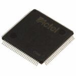 A54SX32A-TQG100
The activity of extra discounts on wholesale prices is in full swing…
Please fill in your contact information and we will send you the latest wholesale price list.



