ChipApex | Global Electronic Components Supplier
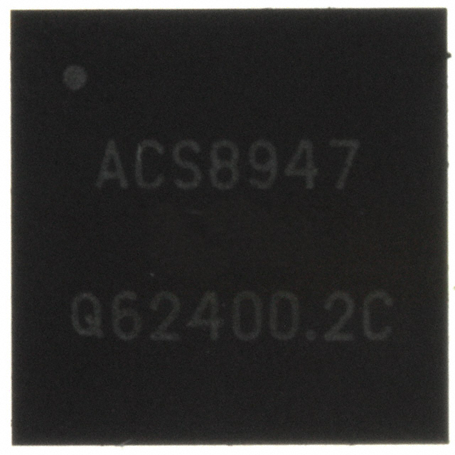
ACS8947T
Search Product
Search Post
— IC芯片 | 连接器 | 传感器 | 被动器件 —
Search productSearch post
— IC芯片 | 连接器 | 传感器 | 被动器件 —
Consult the customer manager about the wholesale price.
consultation hotline:86-132-6715-2157
email:[email protected]
Contact the product manager for consultation. One-stop consultation is available.
Do you want a lower wholesale price? Please send us your inquiry and we will reply immediately.
The ACS8947T is a general-purpose, Integer-N, jitter-attenuating differential phase-locked loop designed for generating low-jitter output clocks. It features two differential LVPECL reference inputs and one differential synchronization input, capable of locking across an input frequency range of 580 kHz to 180 MHz. The device includes four independently supplied differential outputs programmable as LVPECL or CML, supporting maximum frequencies up to 625 MHz. An integrated VCO operates between 2.35 GHz and 2.9 GHz. Configuration is achieved via a hardwired matrix without requiring an external microprocessor.
Verify the specific package variant and temperature rating during acquisition. The datasheet specifies a QFN48 package (7 mm x 7 mm) and operation from -40°C to +85°C. Confirm that the ordering suffix matches the required configuration options, as settings are determined by hardwiring at power-up. Ensure evaluation tools are available for initial setup.
Select this component when a microprocessor-free solution is required for jitter attenuation and frequency translation. The hardwired configuration method suits applications where system complexity must be minimized. Verify that the input frequency range (580 kHz–180 MHz) and output requirements (up to 625 MHz) align with the target design. Consider the need for external loop filter components to customize closed-loop bandwidth.
The ACS8947T belongs to Semtech's Jitter Attenuating Multiplying Phase-Locked Loop (JAM PLL) family. It is positioned as a high-performance clock generator for telecommunications and data communication systems. The device complements other Semtech products like the ACS85xx series by providing robust clock conditioning and synchronization capabilities in a compact form factor.
No direct public substitute part numbers are documented in the provided datasheet. When evaluating alternatives, ensure compatibility with LVPECL/CML interfaces, similar VCO frequency ranges, and comparable jitter performance metrics for SONET/SDH applications.
 ACS8947T
The activity of extra discounts on wholesale prices is in full swing…
Please fill in your contact information and we will send you the latest wholesale price list.