 ChipApex | Global Electronic Components Supplier
SEARCH
Search Product
Search Post
— IC芯片 | 连接器 | 传感器 | 被动器件 —
Search productSearch post
— IC芯片 | 连接器 | 传感器 | 被动器件 —
Consult the customer manager about the wholesale price.
consultation hotline:86-132-6715-2157
email:[email protected]
Contact the product manager for consultation. One-stop consultation is available.
Do you want a lower wholesale price? Please send us your inquiry and we will reply immediately.
The AD10242 is a dual-channel, 12-bit, 40 MSPS monolithic microwave integrated circuit (MMIC) analog-to-digital converter with integrated analog input signal conditioning. Manufactured on the MIL-PRF-38534 line, it integrates two AD9632 amplifiers, two OP279 buffers, and two AD9042 ADCs within a custom 68-lead ceramic gull-wing package. The device operates from ±5.0 V analog supplies and a separate +5.0 V digital supply. It features laser-trimmed channel matching for gain and offset, achieving better than 80 dB channel-to-channel isolation. Key electrical specifications include a guaranteed sample rate of 40 MSPS, an spurious-free dynamic range of 80 dBc at –1 dBFS, and a total power dissipation under 2 W.
Verify that the ordering suffix TZ/883B corresponds to the specific military qualification level required. Confirm the package type is the 68-lead ceramic gull-wing configuration. Ensure compatibility with the ±5.0 V analog and +5.0 V digital supply requirements during system design validation.
Select this component when a complete dual-signal chain solution is required to minimize external discrete components. Choose based on the need for high dynamic range (80 dB SFDR) and precise channel matching in harsh environments. Consider the available input impedance options (50 Ω, 75 Ω, 100 Ω, etc.) by configuring unused analog input pins as ground or resistors.
The AD10242 utilizes internal AD9632, OP279, and AD9042 components within a single MCM to provide space and performance advantages over previous discrete solutions. It is designed for wide dynamic range applications where system complexity reduction is critical. The device allows for AC coupling directly to the ADC by contacting the factory for custom options that bypass the front-end amplifier section.
Publicly confirmed substitute part numbers are not provided in the source documentation. Designers should evaluate pin-compatible alternatives only if they meet the MIL-STD-883B qualification and 68-lead ceramic package constraints.
The input impedance can be selected by using different analog input terminals (AIN1, AIN2, AIN3) or by shorting unused inputs to ground or adding external resistors. For example, AIN1 provides 100 Ω impedance when AIN2 and AIN3 are open, or 50 Ω when AIN2 is shorted to ground.
The ENCODE input supports TTL and CMOS logic. For optimal performance, differential encoding is recommended using an RF transformer or ECL gate. If using single-ended sources, the ENCODE pin should be driven while the complementary ENCODE pin is decoupled to ground with a low-inductance capacitor.
Yes, unipolar operation is supported by adding an external resistor between UPOS and UCOM for positive signals or between UNEG and UCOM for negative signals. Offset calibration is required when configuring for unipolar modes.
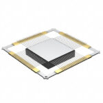 AD10242TZ/883B
The activity of extra discounts on wholesale prices is in full swing…
Please fill in your contact information and we will send you the latest wholesale price list.




