 ChipApex | Global Electronic Components Supplier
SEARCH
Search Product
Search Post
— IC芯片 | 连接器 | 传感器 | 被动器件 —
Search productSearch post
— IC芯片 | 连接器 | 传感器 | 被动器件 —
Consult the customer manager about the wholesale price.
consultation hotline:86-132-6715-2157
email:[email protected]
Contact the product manager for consultation. One-stop consultation is available.
Do you want a lower wholesale price? Please send us your inquiry and we will reply immediately.
The AD13280 is a dual-channel, 12-bit, 80 MSPS analog-to-digital converter (ADC) with integrated analog input signal conditioning. It utilizes a multipass pipeline architecture and laser-trimmed thin-film resistor networks to achieve high channel matching and isolation. The device operates with ±5.0 V analog supplies and a 3.3 V digital supply. Key electrical specifications include a typical Signal-to-Noise Ratio (SNR) of 70 dBFS at 10 MHz input, an 80 dB Spurious-Free Dynamic Range (SFDR), and 90 dB channel-to-channel isolation. Each channel features selectable bipolar input ranges of ±0.5 V or ±1.0 V for single-ended operation and ±1 V for differential inputs.
Verify the specific ordering suffix against the manufacturer's official Ordering Guide to confirm package type and temperature range. Confirm that power supply requirements match the system design, as the device requires separate ±5.0 V analog rails and a 3.3 V digital rail. Ensure thermal management solutions are adequate for the specified power dissipation per channel.
Select this component when a complete, dual-channel ADC solution with built-in front-end amplification is required to minimize external components. Choose based on the necessary analog input impedance (50 Ω, 100 Ω, or 200 Ω) and voltage range. Verify that the system clock source meets the low jitter requirements (<0.3 ps rms) to maintain specified SNR and SFDR performance at 80 MSPS.
The AD13280 belongs to Analog Devices' family of high-speed data converters designed for complex signal processing applications. It integrates custom ADC ICs alongside standard components like the AD8045, AD8138, and AD8031 within a single 68-lead ceramic gull-wing package. This integration allows for significant board area savings while maintaining precise channel matching through laser-trimmed resistor networks.
No direct public substitute part numbers are documented in the provided datasheet. When evaluating alternatives, ensure compatibility with the ±5.0 V analog supply requirement and the 3.3 V digital interface. Verify that replacement devices offer comparable channel-to-channel isolation and integrated signal conditioning if board space reduction is a priority.
The input impedance is determined by the connection of the AMP-IN-X-1 and AMP-IN-X-2 pins. AMP-IN-X-1 provides 100 Ω impedance if AMP-IN-X-2 is open, or 50 Ω if AMP-IN-X-2 is shorted to ground. AMP-IN-X-2 provides 200 Ω impedance if AMP-IN-X-1 is open.
For optimum performance, the AD13280 should be clocked differentially using a low-jitter source. A preferred method involves converting a single-ended clock to differential via an RF transformer, with back-to-back Schottky diodes limiting the differential voltage swing to approximately 0.8 V p-p.
The device supports selectable bipolar input ranges. For single-ended inputs, the ranges are ±0.5 V (using AMP-IN-X-1) and ±1.0 V (using AMP-IN-X-2). For differential inputs (A+IN/A–IN or B+IN/B–IN), the nominal full-scale range is ±1 V.
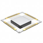 AD13280AF
The activity of extra discounts on wholesale prices is in full swing…
Please fill in your contact information and we will send you the latest wholesale price list.




