 ChipApex | Global Electronic Components Supplier
SEARCH
Search Product
Search Post
— IC芯片 | 连接器 | 传感器 | 被动器件 —
Search productSearch post
— IC芯片 | 连接器 | 传感器 | 被动器件 —
Consult the customer manager about the wholesale price.
consultation hotline:86-132-6715-2157
email:[email protected]
Contact the product manager for consultation. One-stop consultation is available.
Do you want a lower wholesale price? Please send us your inquiry and we will reply immediately.
The AD1674JNZ is a complete monolithic 12-bit analog-to-digital converter manufactured by Analog Devices Inc. It integrates an onboard sample-and-hold amplifier (SHA), a 10 V reference, clock circuitry, and three-state output buffers for microprocessor interfacing. The device operates with +5 V logic supply and ±12 V or ±15 V analog supplies. Key electrical specifications include a sampling rate of 100 kSPS, a full-power bandwidth of 1 MHz, and integral nonlinearity of ±1 LSB. It supports unipolar input ranges of 0 V to +10 V and 0 V to +20 V, as well as bipolar ranges of ±5 V and ±10 V.
Verify the specific temperature grade and package configuration when ordering. The 'J' suffix indicates operation from 0 °C to +70 °C. Confirm that the DIP-28 plastic package matches the design requirements. Ensure power supply rails are within the specified operating voltages of +11.4 V to +16.5 V for VCC and -16.5 V to -11.4 V for VEE.
Select the AD1674JNZ for applications requiring 12-bit resolution at 100 kSPS with integrated signal conditioning. Choose this model over other grades if the operating environment stays within the commercial temperature range of 0 °C to +70 °C. Consider the K-grade variant if tighter integral nonlinearity specifications of ±1/2 LSB are required.
The AD1674 belongs to the AD1674 series of 12-bit ADCs. The JNZ designation specifically refers to the J-grade device in a Plastic DIP-28 package. Other variants include the KNZ (K-grade, Plastic DIP) and JR/R-series (SOIC packages). The device is implemented using BiMOS II process technology.
The AD1674 is pin-compatible with the AD574A and AD674A. When replacing legacy components, verify that the system timing accommodates the AD1674's conversion characteristics. No direct cross-manufacturer substitutes are listed in the provided documentation.
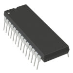 AD1674JNZ
The activity of extra discounts on wholesale prices is in full swing…
Please fill in your contact information and we will send you the latest wholesale price list.




