 ChipApex | Global Electronic Components Supplier
SEARCH
Search Product
Search Post
— IC芯片 | 连接器 | 传感器 | 被动器件 —
Search productSearch post
— IC芯片 | 连接器 | 传感器 | 被动器件 —
Consult the customer manager about the wholesale price.
consultation hotline:86-132-6715-2157
email:[email protected]
Contact the product manager for consultation. One-stop consultation is available.
Do you want a lower wholesale price? Please send us your inquiry and we will reply immediately.
The AD1991ASV is a Class D/1-Bit audio power output stage in a 52-lead TQFP package. It supports stereo BTL or quad single-ended configurations with an 8 V to 20 V power supply range. Output power reaches 20 W at 4 Ω (14.4 V) or 8 Ω (20 V). Efficiency is 87% at 20 W into 8 Ω. On-resistance is 260–320 mΩ per high-side and 190–235 mΩ per low-side transistor. Thermal shutdown activates at 150°C, warning at 135°C. Overcurrent protection triggers above 5 A.
Verify the specific suffix ASV corresponds to the Thin Quad Flat Pack SV-52 package variant. Confirm the industrial temperature range of -40°C to +85°C matches your operational requirements. Ensure proper ESD handling procedures are followed due to device sensitivity. Check datasheet revision status for any updates to absolute maximum ratings or electrical characteristics before finalizing procurement specifications.
Select this component for applications requiring high-efficiency Class D amplification without external MOSFETs. The internal H-bridge architecture simplifies design by integrating power transistors. Consider the exposed pad for thermal management, as heat sinking is critical for maintaining performance under high power loads. Verify that the 5 V analog and digital supply voltages align with your system's logic levels.
This part belongs to Analog Devices' Class D audio power output stage portfolio. It utilizes a low-cost DMOS process to deliver high power density. The device integrates control logic, level shifters, and protection circuits into a single package. It serves as a complete solution for multi-channel audio amplification in consumer and automotive electronics.
The AD1991ASVRL is the reel version of the same component. No other direct substitutes are documented in the provided source material.
Channel mode is determined by the logic level on the MODE1 pin when the RST/PDN signal goes high. A Logic 0 selects 2-channel mode, while a Logic 1 selects 4-channel mode.
In 2-channel mode, ERR0 functions as an active-low data loss error output. It indicates if there are no transitions on the input signals for more than 50 ms, which could cause harmful DC voltage across the load.
Edge speed is set by applying specific logic levels to the ERR3, ERR2, and INB pins while RST/PDN is held low. These settings are latched when RST/PDN rises.
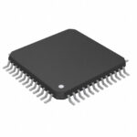 AD1991ASV
The activity of extra discounts on wholesale prices is in full swing…
Please fill in your contact information and we will send you the latest wholesale price list.







