 ChipApex | Global Electronic Components Supplier
SEARCH
Search Product
Search Post
— IC芯片 | 连接器 | 传感器 | 被动器件 —
Search productSearch post
— IC芯片 | 连接器 | 传感器 | 被动器件 —
Consult the customer manager about the wholesale price.
consultation hotline:86-132-6715-2157
email:[email protected]
Contact the product manager for consultation. One-stop consultation is available.
Do you want a lower wholesale price? Please send us your inquiry and we will reply immediately.
The AD2S80ATD is a monolithic resolver-to-digital converter manufactured on a BiMOS II process, housed in a 40-lead DIP package. It provides 10-, 12-, 14-, or 16-bit resolution set by user-selectable control pins SC1 and SC2. The device operates with ±12 V analog supplies and a +5 V logic supply, consuming typically 300 mW. It supports reference frequencies from 50 Hz to 20,000 Hz and offers ratiometric tracking conversion for high noise immunity. Maximum tracking rates range from 16.25 rps at 16 bits to 1040 rps at 10 bits. The industrial temperature grade (AD suffix) ensures operation between -40°C and +85°C.
Verify the ordering suffix 'TD' corresponds to the extended temperature grade (-55°C to +125°C) if required, as the 'AD' suffix denotes the industrial grade (-40°C to +85°C). Confirm package type is 40-lead DIP. Ensure power supply polarity is strictly maintained as +12V and -12V to prevent damage. Check for MIL-STD-883B processing requirements if military qualification is needed.
Select external components R4 and R6 based on the chosen resolution and desired maximum tracking rate. For 10-bit resolution, the maximum tracking rate can reach 1040 rps, while 16-bit resolution limits this to 16.25 rps. Ensure the reference frequency to bandwidth ratio adheres to guidelines: 2.5:1 for 10 bits, up to 7.5:1 for 16 bits. Use preferred value resistors and capacitors with 5% tolerance to maintain performance.
The AD2S80A series includes variants such as AD2S80AJD (commercial), AD2S80ABD (industrial), and AD2S80ATE (extended). The AD2S80ATD specifically refers to the extended temperature grade in a DIP package. Other models like AD2S81AJD offer 12-bit resolution, while AD2S99APZ is an oscillator component often used in similar signal conditioning contexts.
Public confirmed substitute part numbers are not available in the provided documentation. The AD2S80A family shares functional similarities, but specific pin-compatible replacements require separate verification against manufacturer cross-reference lists not included in the source material.
Resolution is set by the logic states of the SC1 and SC2 pins: 0/0 for 10 bits, 0/1 for 12 bits, 1/0 for 14 bits, and 1/1 for 16 bits.
The VELOCITY output provides an analog DC signal proportional to the rate of change of the input angle, which can replace a tachogenerator in servo loops.
Data transfer is managed using INHIBIT, ENABLE, and BYTE SELECT pins. INHIBIT freezes data updates, ENABLE controls output latch state, and BYTE SELECT selects between MSB and LSB bytes on the DB1-DB8 lines.
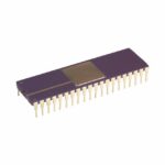 AD2S80ATD
The activity of extra discounts on wholesale prices is in full swing…
Please fill in your contact information and we will send you the latest wholesale price list.





