 ChipApex | Global Electronic Components Supplier
SEARCH
Search Product
Search Post
— IC芯片 | 连接器 | 传感器 | 被动器件 —
Search productSearch post
— IC芯片 | 连接器 | 传感器 | 被动器件 —
Consult the customer manager about the wholesale price.
consultation hotline:86-132-6715-2157
email:[email protected]
Contact the product manager for consultation. One-stop consultation is available.
Do you want a lower wholesale price? Please send us your inquiry and we will reply immediately.
The AD5122AWBCPZ10-RL7 is a dual-channel, nonvolatile digital potentiometer from the AD5122A family. It features two independent 10 kΩ resistors with 128 tap positions and an I²C interface. The device operates on a single supply of 2.3 V to 5.5 V or a dual supply of ±2.25 V to ±2.75 V, with a logic supply range of 1.8 V to 5.5 V. Key electrical parameters include a maximum resistor tolerance of 8%, a temperature coefficient of 35 ppm/°C, and a wiper current capability of ±6 mA for the 10 kΩ variant. It provides a bandwidth of 3 MHz and fast start-up time under 75 µs.
Verify the specific ordering suffix against the manufacturer's official documentation to confirm package type and interface compatibility. Ensure that the 'W' suffix designation aligns with the required ESD protection levels and automotive qualification standards specified in the datasheet.
Select this component when dual-channel adjustment with nonvolatile memory retention is required. The 10 kΩ resistance value and ±6 mA wiper current are suitable for moderate load applications. Verify that the system voltage falls within the 2.3 V to 5.5 V single-supply range or the specified dual-supply limits.
This part belongs to the AD5122A/AD5142A family, which offers both SPI and I²C interface options across different models. The AD5122A specifically denotes the dual-channel, 128-position variant with I²C communication. The 'W' suffix typically indicates automotive-grade qualification and specific ESD ratings compared to commercial variants.
Direct substitutes within the same family include the AD5122BCPZ10-RL7 (SPI interface) or AD5122BRUZ10-RL7 (SPI interface). For I²C interfaces, verify if the AD5122AWRUZ10-RL7 (TSSOP package) meets the physical footprint requirements.
For the 10 kΩ version, the maximum continuous current is ±6 mA. For the 100 kΩ version, it is limited to ±1.5 mA.
When the INDEP pin is enabled, the device enters linear gain setting mode at power-up, allowing independent programming of resistance between terminals RAW and RWB for precise resistor matching.
The typical power dissipation is 3.5 µW when VIH = VLOGIC or VIL = GND.
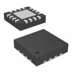 AD5122AWBCPZ10-RL7
The activity of extra discounts on wholesale prices is in full swing…
Please fill in your contact information and we will send you the latest wholesale price list.





