 ChipApex | Global Electronic Components Supplier
SEARCH
Search Product
Search Post
— IC芯片 | 连接器 | 传感器 | 被动器件 —
Search productSearch post
— IC芯片 | 连接器 | 传感器 | 被动器件 —
Consult the customer manager about the wholesale price.
consultation hotline:86-132-6715-2157
email:[email protected]
Contact the product manager for consultation. One-stop consultation is available.
Do you want a lower wholesale price? Please send us your inquiry and we will reply immediately.
The AD5201BRM50 is a single-channel, 33-position digital potentiometer manufactured by Analog Devices. It features a nominal end-to-end resistance of 50 kΩ with a linear taper and a temperature coefficient of 500 ppm/°C. The device operates on a single supply voltage ranging from 2.7 V to 5.5 V or dual supplies of ±2.7 V. It utilizes a 3-wire SPI-compatible serial interface for control, accepting a 6-bit data word. Key electrical characteristics include a wiper resistance of 50 Ω to 100 Ω, shutdown current of 5 µA maximum, and operation within an industrial temperature range of –40°C to +85°C.
Verify the specific ordering suffix 'BRM' confirms the MSOP-10 package and industrial temperature grade (-40°C to +85°C). Confirm the '50' suffix indicates the 50 kΩ nominal resistance value. Ensure compatibility with the 3-wire SPI interface timing requirements, specifically CS setup and hold times, during system integration.
Select this component when a low-resolution, high-resistance digital potentiometer is required for precise analog signal conditioning. The 33 positions may be insufficient for applications requiring finer resolution than the AD5200 (256 positions). Verify that the 50 kΩ end-to-end resistance aligns with the bandwidth and noise requirements, as higher resistance values reduce the -3 dB bandwidth compared to 10 kΩ variants.
The AD5201BRM50 belongs to the AD5200/AD5201 family of programmable resistor devices. While the AD5200 offers 256 positions (8-bit), the AD5201 provides 33 positions (6-bit). Both share identical physical footprints, interfaces, and electrical characteristics except for resolution and internal switch architecture. This part serves as a direct digital replacement for mechanical potentiometers in space-constrained designs.
Public confirmed substitute part numbers are not provided in the source documentation. Designers should verify pinout compatibility and electrical specifications against other Analog Devices digital potentiometers such as the AD5200 series or AD524x series if alternative resolutions or interfaces (e.g., I2C) are acceptable.
The wiper resistance (RW) ranges from 50 Ω to 100 Ω when VDD = 5 V.
When SHDN is driven low, Terminal A becomes an open circuit, and the Wiper (W) is shorted to Terminal B, placing the device in a zero-power consumption state while maintaining the latch contents.
The maximum current (IMAX) is bounded by the switch handling limits and power dissipation, typically specified up to ±20 mA depending on the applied voltage across terminals and resistance setting.
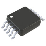 AD5201BRM50
The activity of extra discounts on wholesale prices is in full swing…
Please fill in your contact information and we will send you the latest wholesale price list.





