 ChipApex | Global Electronic Components Supplier
SEARCH
Search Product
Search Post
— IC芯片 | 连接器 | 传感器 | 被动器件 —
Search productSearch post
— IC芯片 | 连接器 | 传感器 | 被动器件 —
Consult the customer manager about the wholesale price.
consultation hotline:86-132-6715-2157
email:[email protected]
Contact the product manager for consultation. One-stop consultation is available.
Do you want a lower wholesale price? Please send us your inquiry and we will reply immediately.
The AD53040KRP is an ultrahigh speed pin driver with a 500 MHz toggle rate and 100 ps edge matching. It features a 50 Ω output impedance, >1.5 V/ns slew rate, and variable output voltages for ECL, TTL, and CMOS logic families. The device operates from +12 V and -7 V supplies, consuming 75 mA per supply. It includes a driver inhibit function to enter a high-impedance state with typically 100 nA leakage current.
Verify the specific RP-20 shipping container option and tube quantity of 38 pieces when sourcing. Confirm that the component meets the required ambient commercial temperature range specifications. Ensure proper heat sinking is employed during handling and installation to maintain compliance with operating temperature limits and prevent permanent damage due to thermal stress.
Select this component for applications requiring direct interface to precision differential ECL timing or single-ended TTL/CMOS sources. Ensure power distribution uses low inductance traces or planes. External bypass capacitors of 0.039 mF are mandatory on VHDCPL and VLDCPL pins to prevent current limiting during full step size transitions. Verify input swing constraints do not exceed 2 V total range among all digital signals.
The AD53040 belongs to Analog Devices' high-speed pin driver portfolio, designed for stimulating digital and mixed-signal test systems. It combines a high-speed monolithic process with a thermally enhanced surface mount package to preserve packaging density. This specific variant provides the necessary performance for real-time stimulation of various logic families in automated testing environments.
No public confirmed substitutes are identified in the provided documentation. When evaluating alternatives, ensure compatibility with the 20-lead SOP package dimensions and thermal characteristics. Verify that replacement devices support the required 500 MHz toggle rate and 50 Ω output impedance specifications.
The driver enters a high-impedance state via the Inhibit Mode, controlled by the INH inputs. In this state, the leakage current is typically 100 nA, and output charge transfer entering inhibit is typically less than 20 pC.
A minimum 0.039 mF capacitor must be connected between VHDCPL and VCC, and another between VLDCPL and VEE. Failure to connect these can cause considerable thermal stress and potential failure of internal current-limiting resistors.
No. Driving with 5V single-ended CMOS exceeds the 2V total range limitation among digital signals. Resistive dividers or equivalent circuitry are required to reduce voltage levels to meet specified timing and performance.
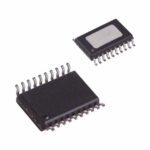 AD53040KRP
The activity of extra discounts on wholesale prices is in full swing…
Please fill in your contact information and we will send you the latest wholesale price list.





