 ChipApex | Global Electronic Components Supplier
SEARCH
Search Product
Search Post
— IC芯片 | 连接器 | 传感器 | 被动器件 —
Search productSearch post
— IC芯片 | 连接器 | 传感器 | 被动器件 —
Consult the customer manager about the wholesale price.
consultation hotline:86-132-6715-2157
email:[email protected]
Contact the product manager for consultation. One-stop consultation is available.
Do you want a lower wholesale price? Please send us your inquiry and we will reply immediately.
The AD537SD is a monolithic voltage-to-frequency converter manufactured by Analog Devices Inc. It integrates an input amplifier, precision oscillator, internal reference generator, and high-current output stage. The device operates from a single supply of 4.5 V to 36 V or dual supplies of ±5 V to ±18 V, consuming 1.2 mA quiescent current. It supports full-scale frequencies up to 150 kHz with nonlinearity as low as 0.07% max at 10 kHz. The AD537SD features a 1.00 V reference output and a 1.00 mV/K absolute temperature reference. Rated for military specifications, it functions within a temperature range of -55°C to +125°C.
Verify the specific suffix 'SD' indicates the ceramic DIP package variant rated for the extended -55°C to +125°C temperature range. Confirm compliance with MIL-STD-883 requirements if applicable to the procurement specification. Ensure external timing components are selected to maintain specified linearity and temperature stability characteristics.
Select the AD537SD when operation in extreme environments below 0°C or above +70°C is required. This model provides superior temperature stability compared to commercial grades. Consider the 14-lead ceramic DIP package for hermetic sealing needs. Evaluate the need for the SYNC pin availability, which is present in the DIP package but absent in metal can variants.
The AD537 series represents a family of high-performance voltage-to-frequency converters designed for precision analog signal processing. The AD537SD specifically denotes the military-grade version housed in a 14-lead side-brazed ceramic DIP package. It shares core architecture with the AD537J and AD537K models but offers extended temperature ratings and enhanced reliability suitable for demanding industrial and aerospace applications.
AD537SH
The DIP package includes a SYNC pin (Pin 2) that allows the internal oscillator to be slaved to an external master oscillator or shut off by connecting to the positive supply.
The open-collector output stage can sink a minimum of 20 mA at a saturation voltage of 0.4 V, with a hard limit of 25 mA.
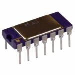 AD537SD
The activity of extra discounts on wholesale prices is in full swing…
Please fill in your contact information and we will send you the latest wholesale price list.





