 ChipApex | Global Electronic Components Supplier
SEARCH
Search Product
Search Post
— IC芯片 | 连接器 | 传感器 | 被动器件 —
Search productSearch post
— IC芯片 | 连接器 | 传感器 | 被动器件 —
Consult the customer manager about the wholesale price.
consultation hotline:86-132-6715-2157
email:[email protected]
Contact the product manager for consultation. One-stop consultation is available.
Do you want a lower wholesale price? Please send us your inquiry and we will reply immediately.
The AD5672RBRUZ is an octal, 12-bit buffered voltage output digital-to-analog converter (DAC) from Analog Devices. It features a low-drift 2.5 V internal reference with a typical temperature coefficient of 2 ppm/°C and operates on a single 2.7 V to 5.5 V supply. The device supports SPI interfaces up to 50 MHz with readback or daisy-chain capabilities and includes user-selectable gain settings for full-scale outputs of 2.5 V or 5 V. Key performance metrics include a maximum integral nonlinearity (INL) of ±1 LSB, a settling time of 8 µs, and power consumption as low as 1.7 µA in power-down mode. It is housed in a 20-lead TSSOP package.
Verify the specific ordering suffix against the manufacturer's current data sheet to confirm package type and temperature grade. Confirm availability status through authorized distributors, as stock levels fluctuate. Ensure compliance with RoHS directives and check for moisture sensitivity level requirements during storage and handling.
Select this component when high channel density and precise voltage output are required. The integrated reference eliminates external components, simplifying design. Verify that the 12-bit resolution meets system accuracy needs and that the 50 MHz SPI speed aligns with the host controller's capabilities. Consider the 2.7 V to 5.5 V supply range for power budgeting.
This part belongs to the nanoDAC+ family, designed for low-power, high-accuracy applications. It shares functional similarities with the AD5676R but offers 12-bit resolution instead of 16-bit. The BRUZ suffix indicates the 20-lead TSSOP package variant. It serves as a multi-channel solution for replacing multiple single-channel DACs in space-constrained designs.
Direct pin-compatible alternatives within the same family include the AD5676R for higher resolution requirements. Other octal DACs may require schematic modifications due to differences in interface protocols or pin assignments. Verify thermal characteristics and power consumption if substituting with devices from other manufacturers.
The device supports serial clock (SCLK) frequencies up to 50 MHz.
Tying the GAIN pin to GND sets the span to 0 V to VREF (2.5 V). Tying it to VLOGIC sets the span to 0 V to 2 × VREF (5 V).
The typical current consumption in all power-down modes is 1.7 µA at temperatures between -40°C and +85°C.
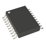 AD5672RBRUZ
The activity of extra discounts on wholesale prices is in full swing…
Please fill in your contact information and we will send you the latest wholesale price list.





