 ChipApex | Global Electronic Components Supplier
SEARCH
Search Product
Search Post
— IC芯片 | 连接器 | 传感器 | 被动器件 —
Search productSearch post
— IC芯片 | 连接器 | 传感器 | 被动器件 —
Consult the customer manager about the wholesale price.
consultation hotline:86-132-6715-2157
email:[email protected]
Contact the product manager for consultation. One-stop consultation is available.
Do you want a lower wholesale price? Please send us your inquiry and we will reply immediately.
The AD5675ACPZ-REEL7 is an octal, 16-bit buffered voltage output digital-to-analog converter (DAC) from Analog Devices. It features a user-selectable gain of 1 or 2 via the GAIN pin, allowing full-scale outputs of VREF or 2 × VREF. The device operates on a single 2.7 V to 5.5 V supply and includes a power-on reset circuit with RSTSEL for zero or midscale initialization. It utilizes a versatile 2-wire I2C-compatible serial interface supporting clock rates up to 400 kHz and 1.8 V logic compatibility. The component is housed in a 20-lead LFCSP package.
Verify the specific grade (A or B) required for your application, as linearity specifications differ between grades. Confirm that the LFCSP-20 package matches your PCB footprint design. Ensure the external pull-up resistor values on the SDA and SCL lines are compatible with the 400 kHz clock rate and bus capacitance limits specified in the timing characteristics.
Select the A Grade variant if tighter integral nonlinearity (±1.8 LSB) is required; otherwise, the B Grade offers ±3 LSB INL. Verify that the reference voltage range supports the desired output span, noting that Gain = 2 requires VREF up to VDD/2. Check thermal resistance requirements for the LFCSP package, specifically the θJA of 82°C/W, to ensure adequate heat dissipation in the target enclosure.
This part belongs to the nanoDAC+ family, which integrates buffered outputs and high-resolution conversion in compact packages. The AD5675 differs from the AD5676 by using an I2C interface instead of SPI. It lacks an internal reference, requiring an external VREF source, unlike the AD5675R variant which includes a 2.5V internal reference.
The AD5675ARUZ is a pin-compatible alternative in a TSSOP-20 package. For SPI interfaces, the AD5676 series serves as a functional equivalent with different communication protocols.
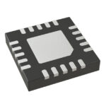 AD5675ACPZ-REEL7
The activity of extra discounts on wholesale prices is in full swing…
Please fill in your contact information and we will send you the latest wholesale price list.





