 ChipApex | Global Electronic Components Supplier
SEARCH
Search Product
Search Post
— IC芯片 | 连接器 | 传感器 | 被动器件 —
Search productSearch post
— IC芯片 | 连接器 | 传感器 | 被动器件 —
Consult the customer manager about the wholesale price.
consultation hotline:86-132-6715-2157
email:[email protected]
Contact the product manager for consultation. One-stop consultation is available.
Do you want a lower wholesale price? Please send us your inquiry and we will reply immediately.
The AD5675ARUZ is an octal, 16-bit buffered voltage output digital-to-analog converter (DAC) from Analog Devices. It features a 2-wire I2C-compatible serial interface and operates on a single 2.7 V to 5.5 V supply. The device includes a user-selectable gain pin for full-scale outputs of VREF or 2 × VREF. Key performance metrics include a maximum integral nonlinearity (INL) of ±8 LSB and a settling time of 8 µs. It supports logic voltages from 1.62 V to 5.5 V and offers power-down modes reducing current consumption to 1 µA typical.
Verify the specific ordering suffix against the manufacturer's official documentation to confirm packaging type and temperature grade. The base model designation indicates standard commercial/industrial specifications; any additional characters may alter electrical parameters or physical form factor. Cross-reference the datasheet revision history to ensure compliance with current design guidelines.
Select this component when multiple high-resolution analog outputs are required within a compact footprint. Ensure the external reference voltage aligns with the desired output span, considering the gain setting. Verify that the system's I2C bus speed does not exceed the specified 400 kHz limit and that the logic voltage range accommodates the microprocessor interface requirements.
This part belongs to the nanoDAC+ family, designed for precision applications requiring low power and high accuracy. It serves as a cost-effective solution for multi-channel signal generation in embedded systems. The device complements other interfaces like SPI through sibling models such as the AD5676 series.
The AD5675RBRUZ is a documented parameter-equivalent alternative offering improved linearity specifications (±3 LSB INL max). Substitution requires verification of pinout compatibility and confirmation that the tighter tolerance meets the application's error budget without necessitating hardware redesign.
The span is determined by the GAIN pin or register bit. Connecting GAIN to GND sets the output range to 0 V to VREF, while connecting it to VLOGIC extends the range to 0 V to 2 × VREF.
The power-on reset circuit ensures all DAC outputs remain at zero scale or midscale until a valid write operation occurs. The specific initial state is selected by tying the RSTSEL pin to GND (zero scale) or VLOGIC (midscale).
Yes, pulsing the LDAC pin low allows any or all DAC registers to update simultaneously if new data exists in the input registers. Alternatively, tying LDAC permanently low enables continuous asynchronous updating.
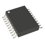 AD5675ARUZ
The activity of extra discounts on wholesale prices is in full swing…
Please fill in your contact information and we will send you the latest wholesale price list.





