ChipApex | Global Electronic Components Supplier
SEARCH
Search Product
Search Post
— IC芯片 | 连接器 | 传感器 | 被动器件 —
Search productSearch post
— IC芯片 | 连接器 | 传感器 | 被动器件 —
Consult the customer manager about the wholesale price.
consultation hotline:86-132-6715-2157
email:[email protected]
Contact the product manager for consultation. One-stop consultation is available.
Do you want a lower wholesale price? Please send us your inquiry and we will reply immediately.
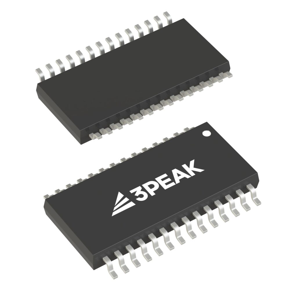
The AD5675BRUZ is an octal, 16-bit buffered voltage output digital-to-analog converter (DAC) from Analog Devices. It operates on a single 2.7 V to 5.5 V supply and features a versatile 2-wire I2C-compatible serial interface with clock rates up to 400 kHz. The device includes a user-selectable gain of 1 or 2 via the GAIN pin, allowing full-scale outputs of VREF or 2 × VREF. It guarantees monotonicity by design and incorporates a power-on reset circuit ensuring outputs initialize to zero or midscale. Power consumption drops to 1 µA typical in power-down mode.
Verify the specific grade suffix (B) against project requirements, as performance parameters such as INL and DNL vary between A and B grades. Confirm package availability, as the component is offered in both 20-lead TSSOP and LFCSP formats. Ensure the selected variant matches the desired thermal and physical footprint constraints for the target PCB layout.
Select the AD5675BRUZ when eight synchronized analog outputs are required within a compact form factor. The internal gain selection feature simplifies reference voltage requirements by allowing span adjustment without external resistors. Verify that the load capacitance does not exceed stability limits, which range from 2 nF to 10 nF depending on the resistive load connected to the outputs.
The AD5675 belongs to the nanoDAC+ family, designed for high-density applications requiring multiple channels. It serves as the I2C-interface counterpart to the SPI-based AD5676. The BRUZ suffix indicates the B-grade performance level packaged in a 20-lead TSSOP housing, distinguishing it from the LFCSP variant and higher-precision A-grade models.
The AD5676RBRUZ offers identical functionality but utilizes an SPI interface instead of I2C. For applications requiring external references, the AD5676 series provides compatible alternatives. Designers must account for interface protocol differences and potential pinout variations when substituting these components.
The gain can be set to 1 or 2 by connecting the GAIN pin to GND or VLOGIC, respectively. This setting determines whether the full-scale output spans 0 V to VREF or 0 V to 2 × VREF.
The outputs power up to either zero scale or midscale, determined by the logic level applied to the RSTSEL pin. Tie RSTSEL to GND for zero scale or to VLOGIC for midscale initialization.
Yes, pulsing the LDAC pin low allows any or all DAC registers to update simultaneously if new data is present in the input registers, ensuring synchronized output changes.
 AD5675BRUZ
The activity of extra discounts on wholesale prices is in full swing…
Please fill in your contact information and we will send you the latest wholesale price list.