ChipApex | Global Electronic Components Supplier
SEARCH
Search Product
Search Post
— IC芯片 | 连接器 | 传感器 | 被动器件 —
Search productSearch post
— IC芯片 | 连接器 | 传感器 | 被动器件 —
Consult the customer manager about the wholesale price.
consultation hotline:86-132-6715-2157
email:[email protected]
Contact the product manager for consultation. One-stop consultation is available.
Do you want a lower wholesale price? Please send us your inquiry and we will reply immediately.
The AD567SD is a high-speed, single-channel, 12-bit digital-to-analog converter (DAC) manufactured by Analog Devices Inc. It features a parallel interface with CMOS and TTL input compatibility and delivers current output. The device operates within a supply voltage range of 11.4 V to 16.5 V and consumes 10 mA of working power. It achieves a settling time of 500 ns and supports both external and internal reference types. The component is housed in a 28-lead SB-CDIP package designed for through-hole mounting and functions reliably across an operating temperature range from -55°C to +70°C.
Verify the specific suffix 'SD' against the official Analog Devices datasheet to confirm pinout and electrical characteristics, as suffixes often denote package type or temperature grade. Confirm RoHS compliance status directly with the manufacturer, as distributor listings may vary. Ensure the parallel interface requirements match the target system's logic levels before procurement.
Select the AD567SD when a single-channel DAC with high speed and parallel connectivity is required. It is suitable for applications needing 12-bit accuracy and current outputs. Consider the 11.4 V to 16.5 V supply requirement and through-hole package constraints during circuit design. Verify that the system can accommodate the parallel data bus width and timing requirements associated with this interface type.
The AD567SD belongs to the AD567 series of high-speed DACs from Analog Devices. This series is characterized by its ability to provide rapid conversion times suitable for demanding real-time applications. The part represents a legacy through-hole solution compared to modern surface-mount nanoDACs, offering robustness for industrial environments where parallel interfaces are preferred for maximum throughput.
Direct replacements must maintain 12-bit resolution, parallel interface, and current output. Check for updated versions in the AD56x family with compatible pinouts. Surface-mount equivalents like the AD5673 require significant PCB redesign due to interface and package differences.
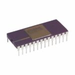 AD567SD
The activity of extra discounts on wholesale prices is in full swing…
Please fill in your contact information and we will send you the latest wholesale price list.