 ChipApex | Global Electronic Components Supplier
SEARCH
Search Product
Search Post
— IC芯片 | 连接器 | 传感器 | 被动器件 —
Search productSearch post
— IC芯片 | 连接器 | 传感器 | 被动器件 —
Consult the customer manager about the wholesale price.
consultation hotline:86-132-6715-2157
email:[email protected]
Contact the product manager for consultation. One-stop consultation is available.
Do you want a lower wholesale price? Please send us your inquiry and we will reply immediately.
The AD5686RBCPZ-RL7 is a quad, 16-bit buffered voltage output Digital-to-Analog Converter (DAC) from the nanoDAC+ family. It integrates a 2.5 V internal reference with a typical drift of 2 ppm/°C and operates on a single 2.7 V to 5.5 V supply. The device features a 50 MHz SPI interface with readback capability and supports 1.8 V logic levels via the VLOGIC pin. Key electrical specifications include a maximum Integral Nonlinearity (INL) of ±2 LSB, a total unadjusted error (TUE) of ±0.1% of Full Scale Range (FSR), and an offset error of ±1.5 mV maximum. It provides a high drive capability of 20 mA and consumes only 3.3 mW at 3 V.
Verify the specific suffix BC in the part number against official documentation to confirm package type and reel configuration. Ensure compatibility with the required operating temperature range of -40°C to +105°C. Confirm that the 16-lead LFCSP footprint matches the PCB layout guidelines provided in the datasheet.
Select this component when a quad-channel DAC with high relative accuracy and low drift is required. The internal 2.5 V reference simplifies design by eliminating external reference components. Consider the 20 mA drive capability for direct load driving without additional amplification. Verify that the 50 MHz SPI speed meets the system's throughput requirements.
This part belongs to the AD5686R/AD5685R/AD5684R family, which shares identical pinouts and interfaces but differs in resolution (16-bit, 14-bit, and 12-bit respectively). The AD5686R is the highest-resolution variant in this series, offering 16-bit precision with the same low-power and compact package options as its lower-resolution counterparts.
Direct functional replacements within the same family include the AD5685R (14-bit) and AD5684R (12-bit) if reduced resolution is acceptable. For external reference variants, consider the AD5686, though it lacks the integrated reference. Ensure any substitute maintains the 16-lead LFCSP package for mechanical compatibility.
When tied to GND, the gain is 1, providing an output range of 0 V to VREF (typically 2.5 V). When tied to VLOGIC, the gain is 2, providing an output range of 0 V to 2 × VREF (typically 5 V).
The RSTSEL pin determines the initial state of the DAC outputs after power-on reset. Tying it to GND powers up all outputs to zero scale, while tying it to VLOGIC powers them up to midscale.
Yes, the SDO (Serial Data Output) pin allows multiple devices to be connected in a daisy chain, enabling data transfer across several units using a single serial bus.
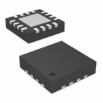 AD5686RBCPZ-RL7
The activity of extra discounts on wholesale prices is in full swing…
Please fill in your contact information and we will send you the latest wholesale price list.






