ChipApex | Global Electronic Components Supplier
SEARCH
Search Product
Search Post
— IC芯片 | 连接器 | 传感器 | 被动器件 —
Search productSearch post
— IC芯片 | 连接器 | 传感器 | 被动器件 —
Consult the customer manager about the wholesale price.
consultation hotline:86-132-6715-2157
email:[email protected]
Contact the product manager for consultation. One-stop consultation is available.
Do you want a lower wholesale price? Please send us your inquiry and we will reply immediately.
The AD5695RBCPZ-RL7 is a quad, 14-bit buffered voltage output digital-to-analog converter (DAC) from the nanoDAC+ family. It integrates a 2.5 V internal reference with a typical drift of 2 ppm/°C and operates on a single 2.7 V to 5.5 V supply. The device features a 400 kHz I2C-compatible serial interface and supports user-selectable gain settings of 1 or 2 via the GAIN pin. Key performance metrics include a maximum total unadjusted error (TUE) of ±0.1% of FSR, a settling time of 5 µs, and low power consumption of 3.3 mW at 3 V. It is housed in a compact 3 mm × 3 mm, 16-lead LFCSP package.
Verify the specific suffix RL7 indicates reel packaging when sourcing. Confirm the B grade designation matches required accuracy specifications. Ensure the LFCSP-16 package footprint aligns with PCB layout guidelines. Check for moisture sensitivity levels and reflow soldering requirements during assembly.
Select this component for applications requiring four independent 14-bit outputs with integrated precision referencing. The I2C interface simplifies microprocessor connections. Consider the 20 mA drive capability and rail-to-rail output swing for direct load interfacing. Verify that the 2.7 V minimum supply voltage meets system power constraints.
This part belongs to the AD5696R/AD5695R/AD5694R family, differentiated primarily by resolution (16-bit, 14-bit, and 12-bit respectively). All variants share identical pinouts, interfaces, and package options. The AD5695R specifically targets mid-range accuracy needs between the 12-bit and 16-bit models while maintaining the same low-power architecture.
The AD5696R and AD5694R are pin-compatible alternatives within the same family, offering 16-bit and 12-bit resolutions respectively. Other nanoDAC+ series devices may require interface or pinout verification before substitution.
The full-scale output is determined by the GAIN pin. Tying GAIN to GND sets a span of 0 V to VREF (typically 2.5 V), while tying it to VLOGIC sets a span of 0 V to 2 × VREF (typically 5 V).
The RSTSEL pin configures the power-on reset behavior. Connecting it to GND forces all DAC outputs to zero scale upon power-up, while connecting it to VLOGIC forces them to midscale.
Yes, the LDAC pin allows asynchronous or synchronous updating. Pulsing LDAC low updates all DAC registers simultaneously if new data is present in the input registers.
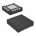 AD5695RBCPZ-RL7
The activity of extra discounts on wholesale prices is in full swing…
Please fill in your contact information and we will send you the latest wholesale price list.