 ChipApex | Global Electronic Components Supplier

SEARCH
Search Product
Search Post
— IC芯片 | 连接器 | 传感器 | 被动器件 —
Search productSearch post
— IC芯片 | 连接器 | 传感器 | 被动器件 —
Consult the customer manager about the wholesale price.
consultation hotline:86-132-6715-2157
email:[email protected]
Contact the product manager for consultation. One-stop consultation is available.
Do you want a lower wholesale price? Please send us your inquiry and we will reply immediately.
The AD5696BRUZ is a quad, 16-bit buffered voltage output digital-to-analog converter (DAC) from the nanoDAC+ family. It operates on a single 2.7 V to 5.5 V supply and features a 400 kHz I2C-compatible serial interface with a VLOGIC pin for 1.8 V logic compatibility. The device guarantees monotonicity by design and offers high relative accuracy with an INL of ±2 LSB maximum at 16 bits. DC performance includes a total unadjusted error (TUE) of ±0.1% FSR maximum and an offset error of ±1.5 mV maximum. It provides a user-selectable gain of 1 or 2 via the GAIN pin, allowing full-scale outputs of 0 V to VREF or 0 V to 2 × VREF respectively.
Verify the specific grade (A or B) required for the application, as specifications such as INL and power consumption vary between grades. Confirm the package type matches the design, as the BRUZ suffix indicates a 16-lead TSSOP package. Ensure the ordering suffix aligns with the desired reel quantity if purchasing in bulk.
Select the AD5696BRUZ when four independent 16-bit channels are required with I2C connectivity. Choose this part over the AD5694 if higher resolution is necessary, noting that the AD5694 is a 12-bit variant. Consider the external reference input requirement, as this model uses an external VREF rather than an internal one. Verify that the load requirements stay within the 2 nF capacitive load stability limit for the chosen gain setting.
The AD5696BRUZ belongs to the nanoDAC+ family, which integrates precision DACs with output amplifiers in small packages. It shares the same functional block diagram and serial interface protocol as other members like the AD5694 and AD5696R, differing primarily in resolution and the presence of an internal reference. The BRUZ designation specifically identifies the 16-lead TSSOP package option.
The AD5696BCPZ-RL7 serves as a direct replacement offering the same electrical characteristics but in a 3 mm × 3 mm LFCSP package instead of the TSSOP. The AD5696ARUZ is available for applications requiring tighter accuracy specifications, such as lower INL and offset errors, while maintaining the same package and interface.
The output range is set by the GAIN pin. When tied to GND, the span is 0 V to VREF. When tied to VLOGIC, the span is 0 V to 2 × VREF.
The RSTSEL pin configures the power-on reset behavior. Tying it to GND forces outputs to zero scale upon power-up, while tying it to VLOGIC forces them to midscale.
Yes, the AD5696 is guaranteed monotonic by design due to its resistor string architecture, with a differential nonlinearity (DNL) of ±1 LSB maximum.
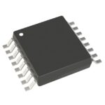 AD5696BRUZ

The activity of extra discounts on wholesale prices is in full swing…
Please fill in your contact information and we will send you the latest wholesale price list.





