ChipApex | Global Electronic Components Supplier

SEARCH
Search Product
Search Post
— IC芯片 | 连接器 | 传感器 | 被动器件 —
Search productSearch post
— IC芯片 | 连接器 | 传感器 | 被动器件 —
Consult the customer manager about the wholesale price.
consultation hotline:86-132-6715-2157
email:[email protected]
Contact the product manager for consultation. One-stop consultation is available.
Do you want a lower wholesale price? Please send us your inquiry and we will reply immediately.
The AD569AD is a monolithic 16-bit digital-to-analog converter manufactured using Analog Devices’ BiMOS II process, combining low-power CMOS logic with high-precision bipolar linear circuitry. It features a voltage-segmented architecture that guarantees 16-bit monotonicity over temperature and time. The device includes double-buffered input latches for flexible 8- or 16-bit bus interfacing and on-chip buffer amplifiers providing a typical settling time of 3 μs to within ±0.001% for a full-scale step. It operates with supply voltages ranging from ±10.8 V to ±13.2 V and is housed in a 28-pin ceramic DIP package.
Verify the specific grade suffix (AD) corresponds to the industrial temperature range of –25°C to +85°C and the 28-pin ceramic DIP package. Confirm that the external reference configuration matches the application's accuracy requirements, as the AD569 requires an external reference voltage typically between ±5 V. Ensure power supplies remain within the specified ±10.8 V to ±13.2 V range to maintain linearity specifications.
Select the AD569AD when 16-bit resolution and guaranteed monotonicity are required in industrial environments. This model is suitable for applications needing fast settling times and buffered voltage outputs. Consider the parallel interface requirements; if serial interfaces are preferred, other members of the nanoDAC family may be more appropriate. Verify that the system can provide the necessary dual power supplies and external reference voltages.
The AD569AD belongs to the AD569 family of 16-bit DACs. Other variants include the AD569JN/KN (commercial plastic packages), AD569BD (industrial ceramic with tighter linearity), and AD569SD (extended temperature ceramic). All share the same core BiMOS II architecture and pinout but differ in temperature ranges and linearity specifications.
Direct pin-compatible replacements within the same family include the AD569BD for improved linearity in the same industrial temperature range. For extended temperature applications, the AD569SD is available. Note that these are legacy components; modern alternatives like the AD569x nanoDAC series offer similar functionality in smaller surface-mount packages but require interface redesign.
Monotonicity is ensured by the voltage-segmented architecture, where buffer amplifiers 'leap-frog' up the first resistor string to preserve monotonicity at segment boundaries, preventing output dips during code transitions.
The on-chip output buffer amplifier can drive capacitive loads of up to 1000 pF without loss of stability.
Yes, the AD569 is designed as a multiplying D/A converter. Its output voltage is proportional to the product of the digital input word and the AC or DC reference voltage applied to the reference terminals.
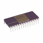 AD569AD

The activity of extra discounts on wholesale prices is in full swing…
Please fill in your contact information and we will send you the latest wholesale price list.