 ChipApex | Global Electronic Components Supplier
SEARCH
Search Product
Search Post
— IC芯片 | 连接器 | 传感器 | 被动器件 —
Search productSearch post
— IC芯片 | 连接器 | 传感器 | 被动器件 —
Consult the customer manager about the wholesale price.
consultation hotline:86-132-6715-2157
email:[email protected]
Contact the product manager for consultation. One-stop consultation is available.
Do you want a lower wholesale price? Please send us your inquiry and we will reply immediately.
The AD630JNZ is a high-precision balanced modulator and demodulator IC from Analog Devices. It utilizes a flexible commutating architecture combined with laser-wafer-trimmed thin-film resistors to achieve high accuracy and temperature stability. The device features two independent differential input stages paired with a precision comparator for low-switching distortion. It supports a supply voltage range of ±5V to ±16.5V and operates within a frequency range of 0Hz to 2MHz. The component is housed in a 20-Lead Standard Small Outline Package (SOIC).
Verify the package type against project requirements, as the AD630JNZ designation typically corresponds to the 20-Lead SOIC variant. Confirm that the operating environment remains within the specified 0°C to 70°C temperature range. Ensure power supply rails are stable between ±5V and ±16.5V to maintain performance specifications. Cross-reference the manufacturer datasheet for specific pinout configurations and electrical characteristics prior to integration.
Select this component when applications require precise amplitude modulation or demodulation with minimal phase error. The internal laser-trimmed resistors reduce the need for external calibration in many fixed-gain scenarios. Consider the 2MHz bandwidth limit when designing for higher-frequency signals. The SOIC package offers a compact footprint suitable for dense circuit board layouts compared to larger DIP alternatives.
The AD630 series represents Analog Devices' solution for high-performance analog signal processing. The JNZ suffix specifically identifies the surface-mount small outline package variant. This part bridges the gap between discrete solutions and complex digital processors, offering an analog approach to coherent detection and signal recovery in noisy environments.
Direct replacements include other AD630 variants such as the AD630JN (DIP package) or AD630SE/883B (military grade), provided the package footprint and lead configuration match the existing PCB design. Verify functional equivalence regarding commutating architecture and gain settings before substitution.
The device is optimized for frequencies up to 2MHz, though it can operate effectively at lower frequencies including DC.
Most common circuits do not require additional external devices due to the integrated application resistor network, though feedback networks may be added for specific gain configurations.
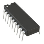 AD630JNZ
The activity of extra discounts on wholesale prices is in full swing…
Please fill in your contact information and we will send you the latest wholesale price list.





