 ChipApex | Global Electronic Components Supplier
SEARCH
Search Product
Search Post
— IC芯片 | 连接器 | 传感器 | 被动器件 —
Search productSearch post
— IC芯片 | 连接器 | 传感器 | 被动器件 —
Consult the customer manager about the wholesale price.
consultation hotline:86-132-6715-2157
email:[email protected]
Contact the product manager for consultation. One-stop consultation is available.
Do you want a lower wholesale price? Please send us your inquiry and we will reply immediately.
The AD650JN is a monolithic voltage-to-frequency and frequency-to-voltage converter manufactured by Analog Devices Inc. It operates with supply voltages ranging from ±9 V to ±18 V and supports full-scale frequencies up to 1 MHz. The device features a typical nonlinearity of 0.002% at 10 kHz and 0.005% at 100 kHz, providing approximately 14-bit linearity. It utilizes a charge balance architecture with separate analog and digital grounds. The component is housed in a 14-lead plastic DIP package and is rated for operation within the commercial temperature range of 0°C to +70°C.
Verify that the specific part number matches the required grade and package configuration. Confirm that the operating environment remains within the specified commercial temperature limits of 0°C to +70°C. Ensure power supply decoupling capacitors are placed close to the pins as recommended for high accuracy designs. Check that input signal ranges do not exceed the absolute maximum ratings defined in the datasheet specifications.
Select this component when high linearity and wide dynamic range are required for signal conditioning. Consider the AD650JN for applications needing simple interfacing to digital logic without additional level shifting. Evaluate the need for separate analog and digital ground planes to minimize noise coupling in sensitive measurement environments. Verify that the required full-scale frequency does not exceed 1 MHz for optimal performance characteristics.
The AD650 series represents a family of precision converters designed for applications requiring high linearity and wide bandwidth. The JN variant specifically denotes the plastic dual in-line package suitable for general commercial use. This model integrates both voltage-to-frequency and frequency-to-voltage conversion capabilities into a single monolithic chip, simplifying circuit design compared to discrete solutions.
No public confirmed substitute part numbers are available in the provided documentation.
The input offset voltage can be trimmed to zero using an external potentiometer connected to the Offset Null pins.
Separate grounds isolate high-precision analog signals from digital switching noise, allowing significant noise on the digital ground without affecting VFC accuracy.
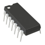 AD650JN
The activity of extra discounts on wholesale prices is in full swing…
Please fill in your contact information and we will send you the latest wholesale price list.





