 ChipApex | Global Electronic Components Supplier
SEARCH
Search Product
Search Post
— IC芯片 | 连接器 | 传感器 | 被动器件 —
Search productSearch post
— IC芯片 | 连接器 | 传感器 | 被动器件 —
Consult the customer manager about the wholesale price.
consultation hotline:86-132-6715-2157
email:[email protected]
Contact the product manager for consultation. One-stop consultation is available.
Do you want a lower wholesale price? Please send us your inquiry and we will reply immediately.
The AD650JP is a monolithic voltage-to-frequency and frequency-to-voltage converter manufactured by Analog Devices Inc. It operates in the commercial temperature range of 0°C to +70°C and is housed in a 20-lead plastic leaded chip carrier (PLCC) package. The device supports full-scale output frequencies up to 1 MHz with typical nonlinearity as low as 0.002% at 10 kHz. It features an open-collector frequency output compatible with TTL or CMOS logic, separate analog and digital ground pins, and user-programmable input ranges via external components.
Verify the specific suffix JP corresponds to the 20-lead PLCC package configuration. Confirm that the commercial temperature rating of 0°C to +70°C meets the operational environment requirements. Ensure that the open-collector output interface is compatible with the target logic family voltage levels. Check for availability of MIL-STD-883 compliant variants if military specifications are required.
Select appropriate external resistors and capacitors to define the full-scale frequency and input voltage range. Consider using larger timing capacitor values to improve linearity performance. Implement proper decoupling capacitors on supply pins to maintain accuracy. Utilize the offset null pins to trim input offset voltage to zero for higher precision applications.
The AD650 series includes various packages such as 14-lead DIP and ceramic options for industrial and extended temperature ranges. The JP variant specifically denotes the surface-mount PLCC package suitable for commercial applications. Other grades like K and B offer tighter linearity specifications compared to J and A grades.
No public confirmed substitute part numbers are available in the provided documentation.
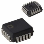 AD650JP
The activity of extra discounts on wholesale prices is in full swing…
Please fill in your contact information and we will send you the latest wholesale price list.





