ChipApex | Global Electronic Components Supplier

SEARCH
Search Product
Search Post
— IC芯片 | 连接器 | 传感器 | 被动器件 —
Search productSearch post
— IC芯片 | 连接器 | 传感器 | 被动器件 —
Consult the customer manager about the wholesale price.
consultation hotline:86-132-6715-2157
email:[email protected]
Contact the product manager for consultation. One-stop consultation is available.
Do you want a lower wholesale price? Please send us your inquiry and we will reply immediately.
The AD664BD-UNI is a monolithic integrated circuit containing four complete 12-bit voltage-output digital-to-analog converters (DACs). It utilizes an R-2R resistor ladder architecture with double-buffered input latches and a data readback function. The device operates with analog supply voltages ranging from ±11.4 V to ±16.5 V and a digital supply of 5 V. Key electrical specifications include a settling time of 10 µs, maximum integral nonlinearity (INL) of ±0.5 LSB, and differential nonlinearity (DNL) of ±0.5 LSB. It features a parallel microprocessor-compatible I/O interface and is housed in a 28-CDIP package.
Verify component authenticity through authorized Analog Devices channels or certified distributors. Confirm lot traceability and MIL-STD-883 compliance if required by specification. Check for lead time variations due to limited production runs. Ensure storage conditions meet moisture sensitivity level requirements prior to assembly.
Select this part for applications requiring four isolated 12-bit outputs with high accuracy. Verify that the 10 µs settling time meets system bandwidth requirements. Ensure the design accommodates the ±11.4 V to ±16.5 V analog supply range. Consider the 28-CDIP package constraints for PCB layout and thermal management.
The AD664BD-UNI belongs to the AD664 family of quad 12-bit DACs. The 'B' suffix typically denotes a specific performance grade or temperature range variant within the series. The 'UNI' suffix often indicates a universal or standard commercial/industrial grade version, distinct from military-compliant variants like the 883B versions. It shares core functionality with other AD664 derivatives but may differ in testing criteria or packaging options.
Direct pin-compatible substitutes within the AD664 family include AD664SD-BIP and AD664JPZ, though package types (CDIP vs PLCC) and specific performance grades must be verified against the original design requirements.
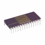 AD664BD-UNI

The activity of extra discounts on wholesale prices is in full swing…
Please fill in your contact information and we will send you the latest wholesale price list.