ChipApex | Global Electronic Components Supplier

SEARCH
Search Product
Search Post
— IC芯片 | 连接器 | 传感器 | 被动器件 —
Search productSearch post
— IC芯片 | 连接器 | 传感器 | 被动器件 —
Consult the customer manager about the wholesale price.
consultation hotline:86-132-6715-2157
email:[email protected]
Contact the product manager for consultation. One-stop consultation is available.
Do you want a lower wholesale price? Please send us your inquiry and we will reply immediately.
The AD7225LN is a monolithic quad 8-bit voltage-output digital-to-analog converter (DAC) fabricated on LC2MOS CMOS technology. It integrates four DACs with output buffer amplifiers and double-buffered interface logic. The device supports single or dual supply operation, featuring separate reference inputs for each channel to allow independent scaling. Key electrical parameters include a maximum settling time of 4 µs, ±1 LSB total unadjusted error (L version), and TTL/CMOS compatible digital inputs. It operates within an extended temperature range of -40°C to +85°C.
Verify the specific package configuration required, as the LN suffix typically denotes a 28-lead PLCC package. Confirm that the L-version specifications meet the accuracy requirements, noting differences in total unadjusted error compared to K/B versions. Ensure power supply rails match the specified ranges for single or dual supply modes to maintain performance guarantees.
Select the AD7225LN when four independent 8-bit channels are required on a single chip. The L-version offers ±1 LSB total unadjusted error, suitable for general-purpose applications. Ensure the design accommodates the minimum VDD to VREF differential of 4V. For bipolar output requirements, external resistors and amplifiers must be added per channel.
The AD7225 belongs to Analog Devices' family of high-speed CMOS DACs. The 'LN' designation specifically identifies the component variant packaged in a 28-lead Plastic Leadless Chip Carrier (PLCC). This package provides a compact surface-mount solution compared to the PDIP or SOIC options available for the same functional core.
Direct pin-compatible replacements within the same package may include other AD7225 variants such as AD7225LPZ, though verification of the specific suffix package type is required. Cross-referencing the absolute maximum ratings and thermal characteristics is necessary when substituting.
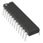 AD7225LN

The activity of extra discounts on wholesale prices is in full swing…
Please fill in your contact information and we will send you the latest wholesale price list.