 ChipApex | Global Electronic Components Supplier

SEARCH
Search Product
Search Post
— IC芯片 | 连接器 | 传感器 | 被动器件 —
Search productSearch post
— IC芯片 | 连接器 | 传感器 | 被动器件 —
Consult the customer manager about the wholesale price.
consultation hotline:86-132-6715-2157
email:[email protected]
Contact the product manager for consultation. One-stop consultation is available.
Do you want a lower wholesale price? Please send us your inquiry and we will reply immediately.
The AD7225LRZ is a monolithic LC2MOS quad 8-bit digital-to-analog converter featuring integrated output buffer amplifiers. It provides four independent voltage outputs with separate reference inputs for each channel, allowing flexible signal conditioning. The device utilizes a double-buffered interface logic compatible with TTL and CMOS levels, enabling simultaneous update of all four outputs via the LDAC pin. It operates from single or dual supplies, typically requiring VDD between 11.4 V and 16.5 V. Key static performance metrics include ±1 LSB total unadjusted error and ±1/2 LSB relative accuracy for the L version. Dynamic characteristics feature a settling time of 4 μs to ±½ LSB and a voltage slew rate of 2.5 V/μs.
Verify the specific suffix 'LRZ' against the manufacturer's current ordering guide to confirm package type and temperature range availability. Ensure supply voltages remain within the specified 11.4 V to 16.5 V range for VDD and -5 V for VSS to maintain guaranteed performance specifications.
Select this component when multiple low-resolution voltage outputs are required on a single chip. The L version offers improved accuracy (±1/2 LSB relative accuracy) compared to K/B versions. Ensure the application can provide separate reference voltages if independent scaling is needed, as internal references are not included.
The AD7225 belongs to Analog Devices' LC2MOS family of data converters, combining high-speed digital logic with precision analog circuitry on a single CMOS process. This integration reduces board space and improves reliability in multi-channel systems. The LRZ designation indicates a specific package variant within the broader AD7225 product line.
Direct replacements within the same family include AD7225KNZ, AD7225CRSZ, and AD7225LPZ. Verify pin compatibility and electrical specifications, particularly the accuracy grade (L vs K/C), before substitution.
Yes, the AD7225 supports single-supply operation using a +15 V VDD supply with VSS connected to AGND. However, dual-supply operation (-5 V VSS) provides better zero-code error and sink capability.
The reference voltage range is from 2 V to (VDD - 4 V). For a typical VDD of 15 V, the maximum reference voltage is 11 V.
Each DAC has an input register and a DAC register. Data is loaded into the selected input register via WR. Simultaneous transfer to all DAC registers occurs on the rising edge of the LDAC signal, ensuring synchronized output updates.
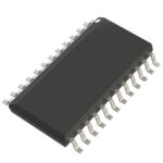 AD7225LRZ

The activity of extra discounts on wholesale prices is in full swing…
Please fill in your contact information and we will send you the latest wholesale price list.






