 ChipApex | Global Electronic Components Supplier

SEARCH
Search Product
Search Post
— IC芯片 | 连接器 | 传感器 | 被动器件 —
Search productSearch post
— IC芯片 | 连接器 | 传感器 | 被动器件 —
Consult the customer manager about the wholesale price.
consultation hotline:86-132-6715-2157
email:[email protected]
Contact the product manager for consultation. One-stop consultation is available.
Do you want a lower wholesale price? Please send us your inquiry and we will reply immediately.
The AD7228ACPZ is an octal 8-bit voltage-mode digital-to-analog converter (DAC) fabricated on LC2MOS technology. It integrates eight DACs with output buffer amplifiers and interface logic on a single chip. The device features individual latches for each channel, controlled via a common 8-bit parallel data bus and address inputs (A0-A2). It operates with dual supplies (VDD: 10.8 V to 16.5 V; VSS: -5 V ± 10%) or a single 15 V supply. Key electrical parameters include a settling time of 5 µs to ±1/2 LSB, differential nonlinearity of ±1 LSB, and a maximum power dissipation of 1 W. The component is housed in a 28-lead PLCC surface-mount package.
Verify the specific suffix 'ACPZ' corresponds to the 28-lead PLCC package variant when sourcing. Confirm that the required operating temperature range aligns with the industrial specification of -40°C to +85°C. Ensure the design accounts for the external reference voltage requirements, as the device utilizes an external VREF pin rather than an internal reference. Check for moisture sensitivity handling requirements associated with the PLCC surface-mount packaging.
Select the AD7228ACPZ when a system requires eight simultaneous 8-bit analog outputs in a compact surface-mount form factor. This model is suitable for applications needing microprocessor-compatible parallel interfaces without complex serial protocols. Designers must provide an external reference voltage between 2 V and 10 V. Consider the 2 kΩ minimum load resistance requirement for the output buffers during circuit layout. Verify that the available board space accommodates the 28-lead PLCC footprint compared to through-hole alternatives.
The AD7228 belongs to Analog Devices' LC2MOS family of octal DACs, designed for high-speed integration of digital logic and precision analog circuits. The ACPZ designation specifically identifies the 28-lead Plastic Leadless Chip Carrier (PLCC) package variant. Other variants in the series include PDIP and SOIC packages, offering flexibility for different mounting styles while maintaining identical functional specifications across the product line.
Direct replacements within the same package and pinout are limited due to the specific LC2MOS process and octal configuration. Evaluate other octal DACs from Analog Devices or competitors if pin compatibility is not strictly required. If a lower channel count suffices, quad-channel DACs may offer cost savings but will require additional board space for multiple units.
Yes, the device supports single 5 V supply operation. However, this mode results in slightly degraded accuracy performance, and the reference voltage must be maintained at approximately 1.23 V to ensure proper functionality.
Each output buffer amplifier is specified to drive a minimum load resistance of 2 kΩ. The buffers are typically tested with a 2 kΩ resistor and 100 pF capacitor load.
Data is transferred into the selected latch on the rising edge of the Write (WR) signal. The A0, A1, and A2 address pins determine which of the eight DAC latches receives the data present on the DB0-DB7 bus when WR goes low.
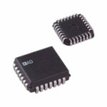 AD7228ACPZ

The activity of extra discounts on wholesale prices is in full swing…
Please fill in your contact information and we will send you the latest wholesale price list.





