 ChipApex | Global Electronic Components Supplier

SEARCH
Search Product
Search Post
— IC芯片 | 连接器 | 传感器 | 被动器件 —
Search productSearch post
— IC芯片 | 连接器 | 传感器 | 被动器件 —
Consult the customer manager about the wholesale price.
consultation hotline:86-132-6715-2157
email:[email protected]
Contact the product manager for consultation. One-stop consultation is available.
Do you want a lower wholesale price? Please send us your inquiry and we will reply immediately.
The AD7228CQ is an octal 8-bit voltage-mode digital-to-analog converter (DAC) fabricated on LC2MOS technology. It integrates eight DACs with output buffer amplifiers and interface logic on a single chip, eliminating the need for external trims. The device features individual latches for each channel, controlled via a common 8-bit parallel data bus and three address lines (A0-A2). It supports both single-supply (13.5 V to 16.5 V) and dual-supply (VDD: 10.8 V to 16.5 V; VSS: -5.5 V to -4.5 V) operation. Key electrical specifications include a settling time of 5 µs to ±1/2 LSB, a maximum power dissipation of 1 W, and an operating temperature range of -40°C to +85°C.
Verify the specific suffix 'CQ' against the manufacturer's current ordering guide, as availability may vary by region. Confirm package type requirements, as the AD7228 family includes PDIP, CERDIP, SOIC, and PLCC variants. Ensure that the design accounts for the 1 W power dissipation limit and appropriate thermal management for the selected package style.
Select the AD7228CQ when eight isolated 8-bit channels are required with buffered outputs. The 'C' grade offers tighter static accuracy (±1 LSB TUE) compared to the 'K' grade (±2 LSB). Choose this component over unbuffered DACs if direct driving of loads up to 2 kΩ is necessary without external amplification. Verify that the system reference voltage falls within the 2 V to 10 V range for optimal performance.
The AD7228 belongs to Analog Devices' LC2MOS family of octal DACs, designed for high-speed integration of digital logic and precision analog circuits. It serves as a multi-channel solution for applications previously requiring multiple discrete converters. The device simplifies board layout by placing all analog inputs/outputs on one side and digital inputs on the other, optimizing trace routing in dense PCB designs.
Publicly confirmed substitute part numbers are not available in the provided documentation. When evaluating alternatives, ensure compatibility with the 8-bit resolution, parallel interface protocol, and ±1 LSB linearity specifications. Verify that replacement devices support the same supply voltage ranges and package dimensions if pin-for-pin substitution is required.
The minimum load resistance is 2 kΩ when the output voltage is 10 V. The output buffer amplifiers are tested with a 2 kΩ load and 100 pF capacitance.
In single-supply operation, the negative-going settling time to voltages near 0 V is slightly longer than in dual-supply operation due to reduced sink capability as the output voltage approaches the ground rail.
Yes, the device can operate from a single 5 V supply. However, this results in slightly degraded accuracy performance, and the reference voltage must be limited to maintain the required overhead voltage between VDD and VREF.
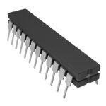 AD7228CQ

The activity of extra discounts on wholesale prices is in full swing…
Please fill in your contact information and we will send you the latest wholesale price list.






