ChipApex | Global Electronic Components Supplier

SEARCH
Search Product
Search Post
— IC芯片 | 连接器 | 传感器 | 被动器件 —
Search productSearch post
— IC芯片 | 连接器 | 传感器 | 被动器件 —
Consult the customer manager about the wholesale price.
consultation hotline:86-132-6715-2157
email:[email protected]
Contact the product manager for consultation. One-stop consultation is available.
Do you want a lower wholesale price? Please send us your inquiry and we will reply immediately.
The AD7247ATQ is a dual 12-bit voltage-output digital-to-analog converter (DAC) from the AD7237A/AD7247A family, manufactured by Analog Devices. It integrates two CMOS DACs with on-chip output amplifiers and a Zener voltage reference on a single monolithic LC2MOS chip. The device features a parallel loading structure for direct microprocessor interfacing. It supports operation from +12 V to +15 V supplies with optional negative supply rails of 0 V or -12 V to -15 V. Key electrical parameters include a maximum settling time of 10 µs, a typical power dissipation of 165 mW in single-supply mode, and an extended temperature range of -55°C to +125°C.
Verify the specific suffix 'TQ' indicates the ceramic DIP package and extended temperature rating. Confirm RoHS compliance status as older manufacturing runs may vary. Check for discontinuation notices or lifecycle status through official Analog Devices channels prior to procurement planning.
Select the AD7247ATQ over the AD7237ATQ when a simple parallel 12-bit latch interface is preferred over the double-buffered 8-bit bus structure. Ensure the application requires the extended -55°C to +125°C operating range provided by the 'T' grade. Verify that the 24-pin CDIP package fits the target PCB layout constraints.
The AD7247ATQ is part of the enhanced AD7237A/AD7247A series, which improves upon the original industry-standard AD7237/AD7247 parts. These enhancements include faster interface times, improved reference variations with supply voltage, and wider power supply operation ranges. The 'T' designation specifies the military-grade temperature range, while 'Q' denotes the hermetic ceramic dual-in-line package.
The AD7247ABR serves as a lower-temperature alternative if the extended range is not required. For applications needing an 8-bit bus interface, the AD7237ATQ is the functional equivalent within the same package and temperature grade.
The output range is set by connecting the ROFS pin: to VOUT for 0-5V, to GND for 0-10V, or to REF IN for ±5V bipolar operation.
The maximum settling time to within ±1/2 LSB is 10 µs for both positive and negative full-scale changes.
Yes, the REF OUT pin provides the internal 5 V reference, capable of sourcing up to 500 µA to external loads.
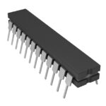 AD7247ATQ

The activity of extra discounts on wholesale prices is in full swing…
Please fill in your contact information and we will send you the latest wholesale price list.